Duty-cycle-efficent SRAM cell test

A storage unit and storage structure technology, applied in static memory, digital memory information, information storage, etc., can solve problems such as device failure, difficulty in detecting bit line contact resistance, and failure to detect defects, etc.

Inactive Publication Date: 2004-08-04
INT BUSINESS MASCH CORP
View PDF1 Cites 3 Cited by
  • Summary
  • Abstract
  • Description
  • Claims
  • Application Information

AI Technical Summary

Problems solved by technology

Slightly increased bitline contact resistance is difficult to detect with existing technologies because even with extremely high bitline contact resistance values, writes to and reads from memory cells can be performed initially
When these increased bit line contact resistance devices are used by consumers, they are subject to additional thermal cycles, shock cycles, etc., and their resistance tends to increase, which causes the device to fail
Therefore, initial testing immediately after manufacture may not detect defects that arise only after the device has been subjected to actual consumer use for some time

Method used


Image

  • Duty-cycle-efficent SRAM cell test
  • Duty-cycle-efficent SRAM cell test
  • Duty-cycle-efficent SRAM cell test

Examples


Embodiment Construction

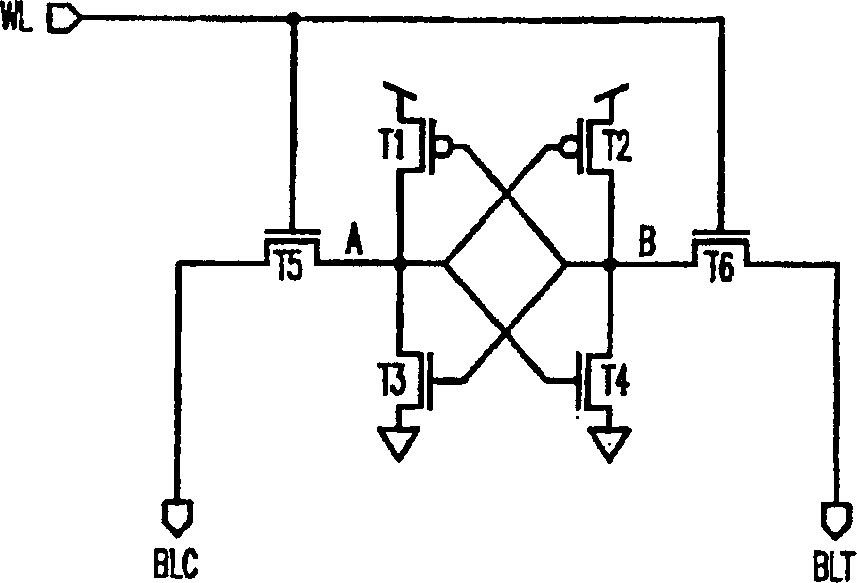
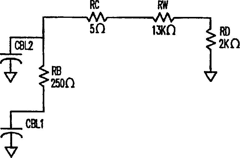
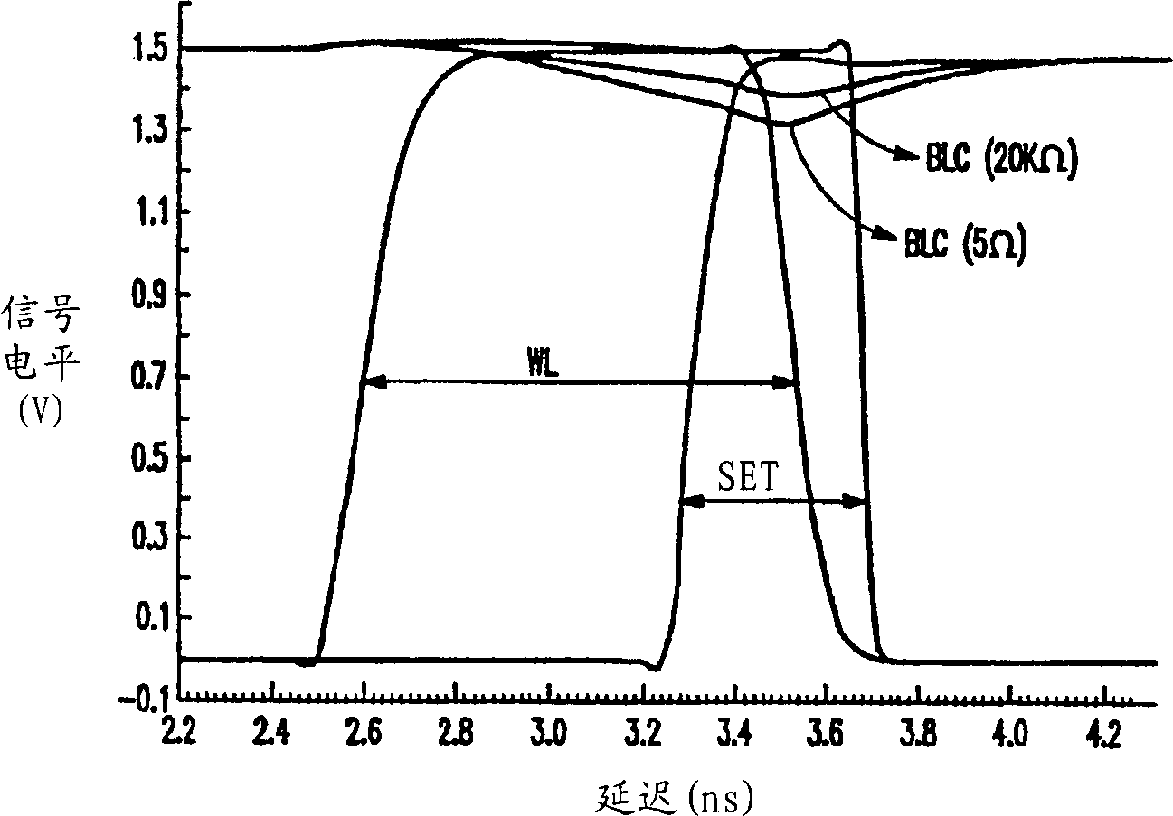
[0027] As mentioned above, there is a need to identify bitline contacts whose resistance values ​​are even marginally higher than optimal. It is difficult for the prior art to detect slightly increased bit line contact resistance, because even with extremely high bit line contact resistance values, the write activity to and the read activity from the memory cell can be performed initially. However, initial testing performed immediately after manufacture may not detect defects that develop only after the device has been subjected to actual consumer use for some time.

[0028] The invention described below overcomes these problems by providing a structure and method that provides substantial stress to the bit line contacts. This allows those bit line contacts which are initially acceptable only on the edges (and which may become defective after some time of use) to be directly identifiable immediately after manufacture. More specifically, the present invention provides a test m...


PUM


Abstract

A method and structure for the invention includes an integrated memory structure having a built-in test portion. The integrated memory structure has memory cells, bitlines and wordlines connected to the memory cells, wordline decoders connected to a plurality of the wordlines, bitline restore devices connected to the bitlines for charging the bitlines during read and write operations, and a clock circuit connected to the wordlines. During a test mode the wordline decoders simultaneously select multiple wordlines that the bitline restore devices maintain in an active state and the clock circuit maintains the multiple wordlines and the bitline restore devices in an active state for a period in excess of a normal read cycle. The invention also includes transistors which are connected to the memory cells. The transistors include bitline contacts which are stressed during the test mode.

Description

technical field [0001] The present invention relates generally to the testing of semiconductor memory cells, and in particular to improved methods and structures for stressing and testing contacts within semiconductor structures. Background technique [0002] A typical semiconductor static random access memory (SRAM) device includes a plurality of word lines, a pair of bit lines and memory cells, wherein cell latches and pass devices are connected between the word lines and the pair of bit lines the intersection between. The pass devices of the memory cells are connected to the pair of bit lines through bit line contacts. These bit line contacts allow the contents of the memory cell to be successfully read from and written to the cell latch during a read or write operation. A bitline contact with too much resistance (resistive bitline contact) will not properly allow reading or writing of the memory cell. Resistive bitline contacts can occur as a result of mechanical fail...

Claims


Application Information

Patent Timeline
Patent Type & Authority Applications(China)
IPC IPC(8): G11C11/413G11C29/06G11C29/28G11C29/34
CPCG11C29/34G11C29/28G11C29/00
Inventor 吉斯莱恩·英伯特德特雷米奥利斯帕斯卡尔·坦霍夫
Owner INT BUSINESS MASCH CORP
Why Eureka
Try Eureka