Electron emitter and method for fabricating the same, cold cathode field electron emission element and method for fabricating the same, and cold cathode field electron emission display and method

A field electron emission and electron emitter technology, applied in cold cathode manufacturing, electrode system manufacturing, discharge tube/lamp manufacturing, etc., can solve the growth obstruction of carbon nanotube structures and the electron emission efficiency of carbon nanotube structures decline, difficulty, etc.

Inactive Publication Date: 2004-09-29
SONY CORP
View PDF0 Cites 7 Cited by
  • Summary
  • Abstract
  • Description
  • Claims
  • Application Information

AI Technical Summary

Problems solved by technology

Therefore, in the above-mentioned step (5), when the carbon nanotube structure is uniformly formed on the negative electrode exposed at the bottom of the opening by the plasma CVD method, it will be difficult if the display device has a large area, and , Damage may occur on field emission components such as gate electrodes, openings, and cathode electrodes that have already been formed.
In addition, when forming a carbon nanotube structure by the plasma CVD method, if an inexpensive glass substrate is used, the formation temperature needs to be lowered to a very low level (below 550°C), but carbon nanotubes will be produced at such a formation temperature. Deterioration of the crystallinity of the structure
On the other hand, if the forming temperature is to be kept at a high temperature, a high-temperature-resistant substrate such as ceramic must be used, which increases the cost
In addition, there is also a problem that the growth of the carbon nanotube structure is hindered due to the influence of outgassing from the insulating layer during the formation process
However, when such a countermeasure is adopted, there is a problem that it is difficult to form a high electric field intensity near the carbon nanotube structure, resulting in a decrease in the electron emission efficiency of the carbon nanotube structure.
However, in this method, since the carbon nanotube structure is buried in the binder material, there is a problem that the electron emission efficiency of the carbon nanotube structure decreases.

Method used


Image

  • Electron emitter and method for fabricating the same, cold cathode field electron emission element and method for fabricating the same, and cold cathode field electron emission display and method
  • Electron emitter and method for fabricating the same, cold cathode field electron emission element and method for fabricating the same, and cold cathode field electron emission display and method
  • Electron emitter and method for fabricating the same, cold cathode field electron emission element and method for fabricating the same, and cold cathode field electron emission display and method

Examples


Embodiment 1

[0123] Embodiment 1 relates to the electron emitter of the present invention, the manufacturing method of the electron emitter related to the first embodiment of the present invention, the cold cathode field electron emission device (hereinafter referred to simply as the field emission device) of the first embodiment and its manufacturing method And the so-called two-electrode type cold cathode field electron emission display device of the first form (hereinafter, simply referred to as a display device) and its manufacturing method also relate to a first method.

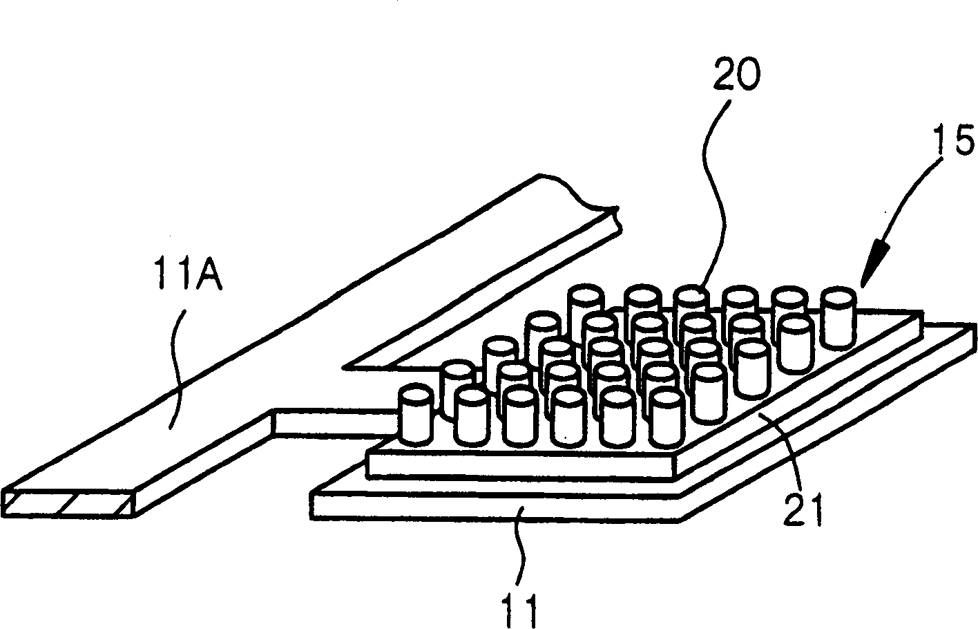
[0124] figure 1 A schematic cross-sectional view of a part of the display device in Example 1 is shown, figure 2 A schematic perspective view of an electron-emitting portion is shown, and (B) of FIG. 4 shows a schematic cross-sectional view of a part of an electron-emitting portion.

[0125] The electron emitter in Example 1 is composed of a matrix 21 and a carbon nanotube structure embedded in the matrix 21 with i...

Embodiment 2

[0178] Embodiment 2 relates to the electron emitter of the present invention, the manufacturing method of the electron emitter of the first aspect of the present invention, the field emission device of the second aspect and its manufacturing method, and the so-called three-electrode display device of the second aspect and its manufacturing method. The manufacturing method also relates to the first method.

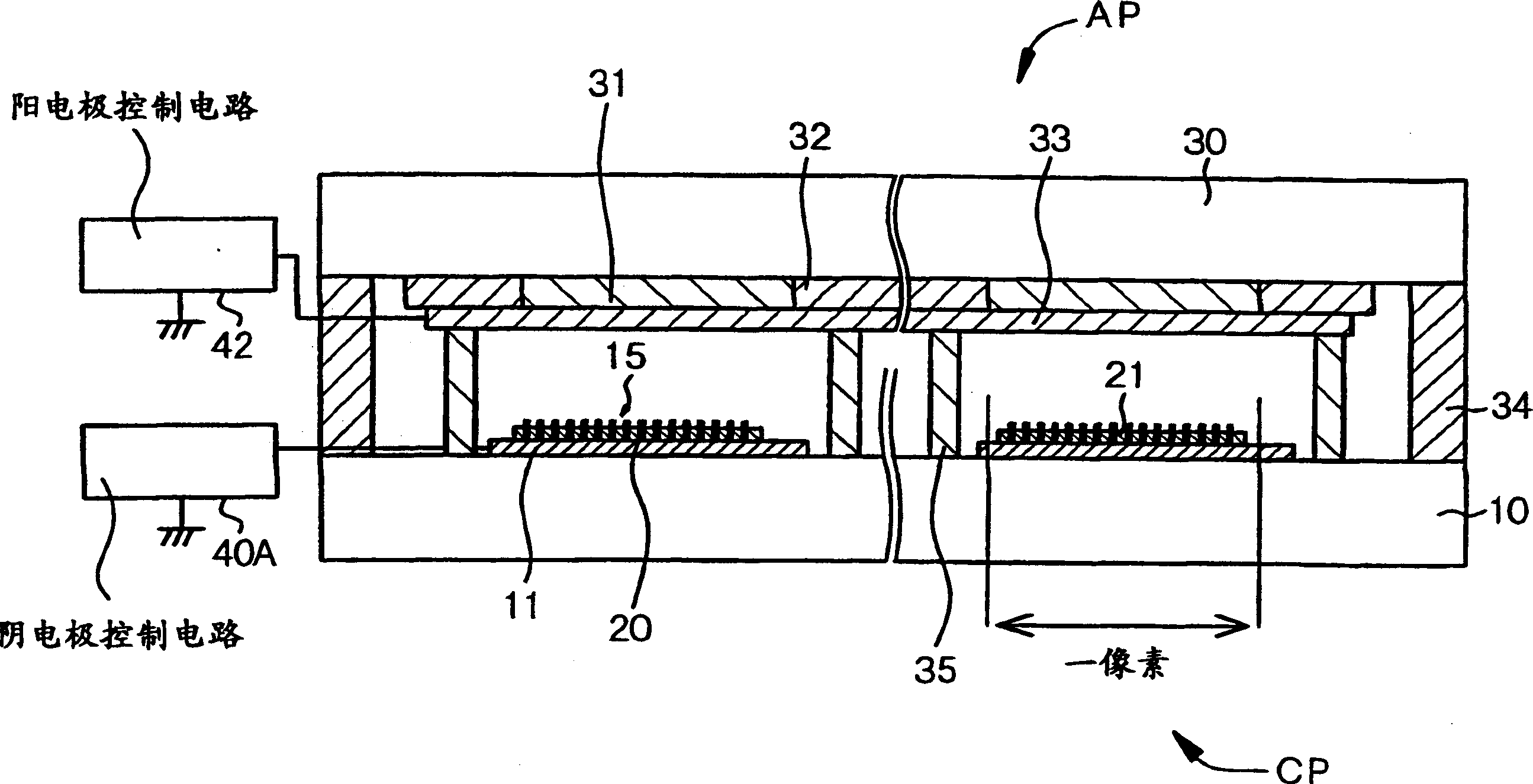
[0179] (B) in FIG. 10 shows a partial schematic end view of the field emission device in Example 2, Figure 7 shows a partial schematic end view of the display device, Figure 8 It shows a partial schematic perspective view when the cathode panel CP and the anode panel AP are disassembled. This field emission component is made up of following parts: the negative electrode 11 (corresponding to substrate) that is formed on the support body 10; The insulating layer 12 that is formed on the support body 10 and the negative electrode 11; The gate electrode that is formed on the...

Embodiment 3

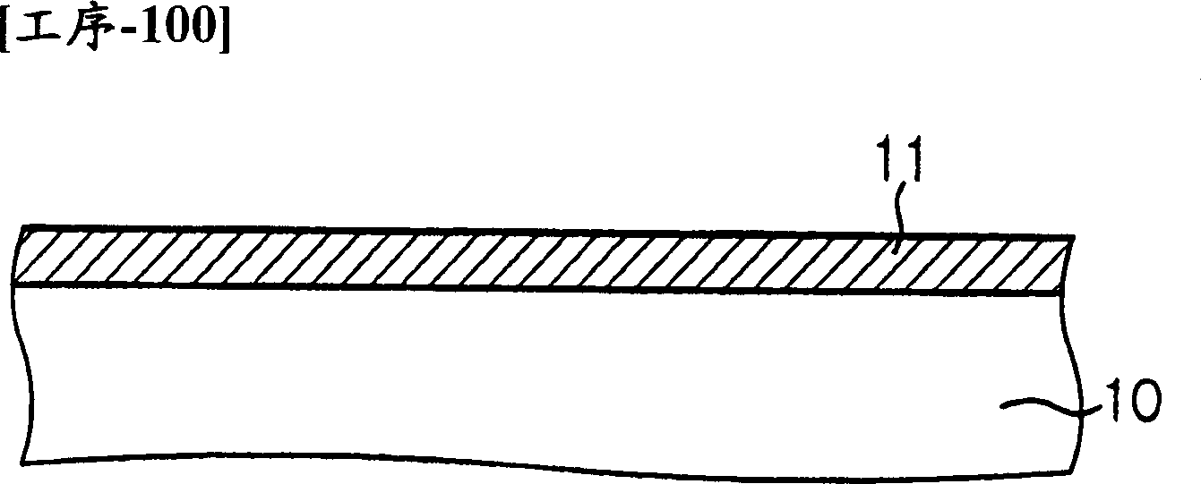
[0202] Embodiment 3 is a modified example of Embodiment 2. Embodiment 3 differs from Embodiment 2 in that carbon nanotubes are formed on the cathode electrode 11 (substrate) by plasma CVD. That is, Embodiment 3 is related to the second method. Hereinafter, a method of manufacturing an electron emitter, a method of manufacturing a field emission member, and a method of manufacturing a display device in Example 3 will be described with reference to (A) and (B) in FIG. 11 .

[0203] [Process-300]

[0204] First, the cathode electrode 11 on which the selective growth region 23 has been formed is formed in the surface region where the electron emission portion is to be formed. Specifically, a mask layer made of a resist material is formed on a support 10 made of, for example, a glass substrate. A mask layer is formed to cover the support 10 other than the portion where the stripe-shaped negative electrodes are to be formed. Next, after forming an aluminum (Al) layer over the en...


PUM


Abstract

A cold cathode field emission device comprises; a cathode electrode 11 formed on a supporting member 10, an insulating layer 12 formed on the supporting member 10 and the cathode electrode 11, a gate electrode 13 formed on the insulating layer 12, an opening portion 14A, 14B formed through the gate electrode 13 and the insulating layer 12, and an electron emitting portion 15 formed on the portion of the cathode electrode 11 positioned in the bottom portion of the opening portion 14B, and said electron emitting portion 15 comprises a matrix, 21 and carbon nanotube structures 20 embedded in the matrix 21 in a state where the top portion of each carbon nanotube structure is projected.

Description

technical field [0001] The invention relates to an electron emitter and its manufacturing method, a cold cathode field electron emission component and its manufacturing method, and a cold cathode field electron emission display device and its manufacturing method. Background technique [0002] In recent years, carbon crystals and carbon nanofibers called carbon nanotubes having a tube structure in which carbon graphite sheets are rolled have been discovered. The diameter of carbon nanotubes is about 1 nm to 200 nm. Known are: single-layer carbon nanotubes with a structure rolled by one layer of carbon graphite sheets and multilayer carbon nanotubes with a structure rolled by more than two layers of carbon graphite sheets carbon nanotubes. No other crystals have been found to be comparable to this crystal with a nanometer-sized tube structure, thus establishing its status as a special substance. In addition, carbon nanotubes have the property of becoming a semiconductor or ...

Claims


Application Information

Patent Timeline
Patent Type & Authority Applications(China)
IPC IPC(8): H01J1/304H01J9/02H01J29/04H01J31/12
CPCH01J2201/30469H01J1/3044H01J31/127H01J1/304B82Y10/00H01J9/025C01B32/05H01J9/02B82Y40/00
Inventor 八木贵郎岛村敏规
Owner SONY CORP
Why Eureka
Try Eureka