Photonic chip mounting in a recess for waveguide alignment and connection

Inactive Publication Date: 2005-05-03
HO SENG TIONG
View PDF10 Cites 64 Cited by
  • Summary
  • Abstract
  • Description
  • Claims
  • Application Information

AI Technical Summary

Benefits of technology

[0029]According to yet another aspect of the present invention, the depth of the recess may be controlled by using as the substrate a silica-on-silicon (SOS) wafer. The thickness of the top silica layer may

Problems solved by technology

Obviously, this approach will not be cost-effective when the semiconductor based photonic chip has a large number of ports (e.g., more than 16).
Because indium-phosphide based materials are expensive and difficult to work with, single-substrate fabrication strategies are not practical for mass-production applications.
But the recess technology has a number of limitations.
For instance, the cleaving process cannot produce a photonic chip with a size controlled to submicron precision because of the relatively large size (typically a few microns) of the diamond tip that initiates the cleaving and the limited positioning precision (about 5 microns) of existing cleaving machinery.
Thus, the method is limited to a photonic chip having only one output (or input) port on one side that must be connected and aligned with one channel waveguide.
For photonic chips having input and output ports on both sides of the chip, as future applications will require, these designs are inadequate

Method used


Image

  • Photonic chip mounting in a recess for waveguide alignment and connection
  • Photonic chip mounting in a recess for waveguide alignment and connection
  • Photonic chip mounting in a recess for waveguide alignment and connection

Examples


Embodiment Construction

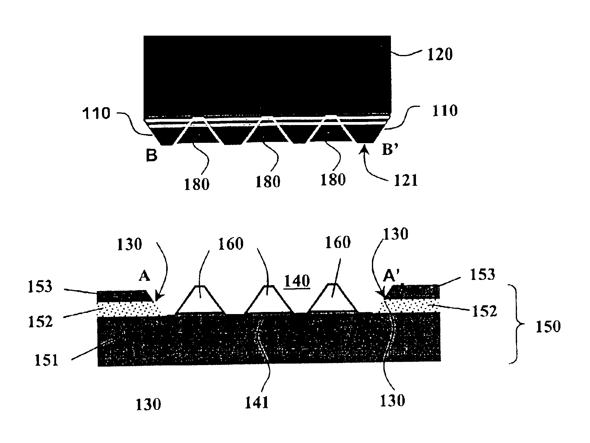
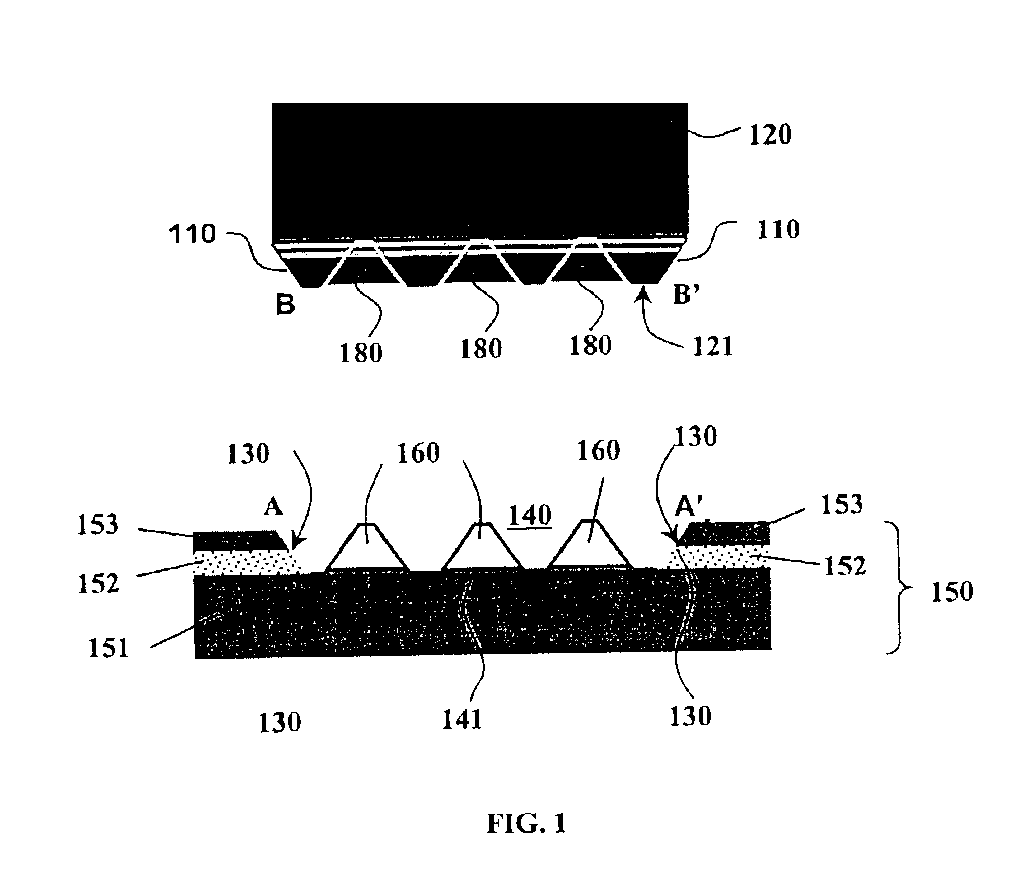
[0039]FIG. 1 is a cross-sectional view of an exemplary embodiment of a photonic chip mounting arrangement according to the present invention. Recess 140 is formed in top layer 153 and insulating (SiO2) layer 152 of silicon-on-insulator (SOI) or silica-on-silicon (SOS) substrate 150. End walls 130 of recess 140 have a nonzero (preferably greater than 10°) inclination angle with respect to vertical; the specific choice of inclination angle will be discussed in more detail below. In some embodiments, all side walls of recess 140 have similarly inclined surfaces, although this is not required. Recess 140 has a substantially flat bottom surface 141. In one embodiment, bottom surface 141 has a surface area of about 300 μm by 300 μm. In one preferred embodiment, a number of pillars 160 (which may be anywhere from 2 to 50 μm tall) are formed on bottom surface 141, each pillar having inclined side faces. Preferably, three pillars 160 in a triangular arrangement are used, but the number and p...


PUM


Abstract

A coupling system for photonic integrated circuits and integrated optical waveguides is provided. A recess is formed in a substrate on which one or more integrated optical waveguides are disposed, the recess being located at the desired mounting location of the photonic integrated circuit. At least one end wall of the recess is inclined with respect to a normal to the substrate surface. At least one end face of a photonic integrated circuit is inclined to match the inclined end wall of the recess. The length, width, and depth of the recess are controlled so that inserting the photonic integrated circuit into the recess passively provides both lateral and vertical alignment of the photonic integrated circuit with the integrated optical waveguide(s).

Description

CROSS-REFERENCES TO RELATED APPLICATIONS[0001]This application claims the benefit of U.S. Provisional Application No. 60 / 339,131, filed Dec. 11, 2001, entitled “Photonic Chip Mounting in a Recess for Waveguide Alignment and Connection,” which disclosure is incorporated herein by reference for all purposes.[0002]This application is related to commonly assigned co-pending U.S. patent application Ser. No. 10 / 083,674, entitled “Integrated Planar Composite Coupling Structures for Bi-directional Light Beam Transformation between a Small Mode Size Waveguide and a Large Mode Size Waveguide,” filed Oct. 19, 2001, the disclosure of which is hereby incorporated by reference for all purposes.[0003]This application is also related to commonly assigned co-pending U.S. patent application Ser. No. 60 / 339,135, entitled “Connection Between a Waveguide Array and a Fiber Array,” filed concurrently herewith, the disclosure of which is hereby incorporated by reference for all purposes.BACKGROUND OF THE I...

Claims


Application Information

Patent Timeline
IPC IPC(8): G02B6/26G02B6/12G02B6/36G02B6/42
CPCG02B6/3636G02B6/423G02B2006/12176G02B6/3692
Inventor ZHOU, YANHO, SENG-TIONG
Owner HO SENG TIONG
Why Eureka
Try Eureka