Method for mfg. semiconductor device

A manufacturing method and semiconductor technology, applied in semiconductor/solid-state device manufacturing, semiconductor devices, construction components on-site preparation, etc., can solve the problems of vertical MOSFET area increase and gate insulating film withstand voltage reduction

Inactive Publication Date: 2004-10-13
SEIKO INSTR INC
View PDF1 Cites 0 Cited by
  • Summary
  • Abstract
  • Description
  • Claims
  • Application Information

AI Technical Summary

Problems solved by technology

[0008] By performing tapered etching on the trench 6, the problem of lower withstand voltage of the gate i

Method used


Image

  • Method for mfg. semiconductor device
  • Method for mfg. semiconductor device
  • Method for mfg. semiconductor device

Examples


Embodiment 1

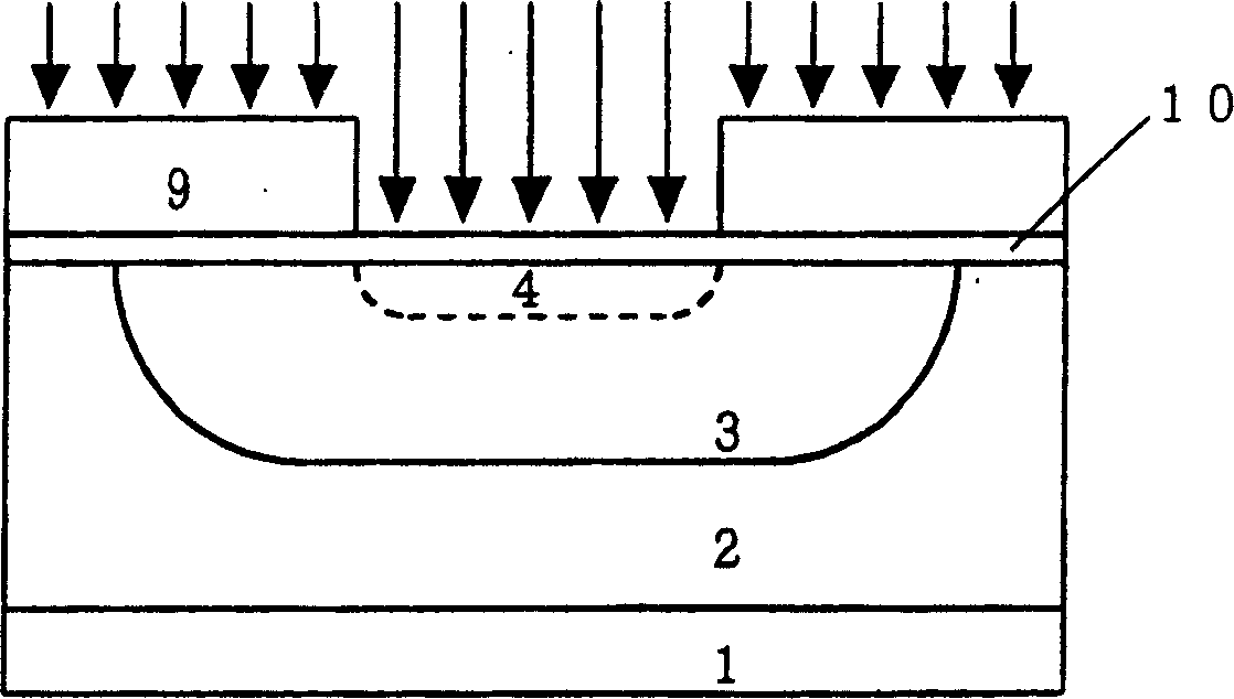
[0030] FIG. 1 is a schematic cross-sectional defect showing a first embodiment of a method of manufacturing a semiconductor device of the present invention. In Fig. 1 (a), on the N+ type semiconductor substrate 1, that is, for example doped with arsenic, the resistivity is 1mΩcm~10mΩcm on the semiconductor substrate of the impurity concentration, form N-semiconductor substrate 2, that is for example doped with phosphorus A semiconductor substrate with a resistivity of 0.1Ωcm to 1Ωcm impurity concentration, on the N-semiconductor substrate 2, for example, ion implantation method with 1 × 10 16 atom / cm 3 ~1×10 18 atom / cm 3 Impurity concentration of boron is implanted to form P- diffusion layer 3 . After the ion implantation, heat treatment for diffusing the P − diffusion layer 3 to a desired depth is performed. After the above-mentioned heat treatment, a photoresist 9 for forming the N-diffusion layer 4 is formed, and the ion implantation method is used to form a 1×10 17 at...


PUM


Abstract

Provided is a manufacturing method for realizing a low cost and high performance vertical MOSFET. The vertical MOSFET manufacturing method of the present invention gives the portion formed between the trench and the semiconductor substrate flat portion a smooth shape by doping the semiconductor substrate with an impurity through ion implantation and then thermally oxidizing the substrate. The withstand voltage of the gate insulating film is thus improved. Furthermore, the semiconductor device manufacturing method of the present invention puts the formation of the N+ diffusion layer serving as a source after the formation of the trench and the subsequent formation of the gate electrode in the trench, and therefore can avoid re-diffusion of the N+ diffusion layer, which otherwise causes an increase in leak current.

Description

technical field [0001] The invention relates to a method for manufacturing a semiconductor device, in particular to a method for manufacturing a vertical MOSFET with a trench structure. Background technique [0002] Now based on the vertical MOSFET as Figure 5 Describe the prior art. The semiconductor substrate has a P-type diffusion layer 3 on its surface, an N-type semiconductor substrate 2 on its lower part, and an N+ type semiconductor substrate 1 below it. Trench 6 is formed at a depth beyond P-type diffusion layer 3 and reaches N-type semiconductor substrate 2 . A gate insulating film 7 is formed on the surface of the trench 6 , and a gate electrode 8 made of polysilicon or the like is embedded therein. Then, an N+ type diffusion layer 5 is provided in the P − type diffusion layer 3 (for example, refer to Patent Document 1). [0003] exist Figure 5 of vertical MOSFETs. Between the N+ semiconductor substrate 1 (high-concentration drain) and N- semiconductor substr...

Claims


Application Information

Patent Timeline
IPC IPC(8): H01L21/336H01L29/423H01L29/78
CPCH01L29/4232H01L29/4238H01L29/7813E04G17/0654E02D29/02
Inventor 小岩进雄
Owner SEIKO INSTR INC
Why Eureka
Try Eureka