Method and apparatus for controlling thickness uniformity of electroplated layers

A technology of anode device and power supply, which is applied in the field of electrodeposition processing and can solve problems such as copper thickness

Inactive Publication Date: 2004-12-01
纽仪器股份有限公司
View PDF15 Cites 22 Cited by
  • Summary
  • Abstract
  • Description
  • Claims
  • Application Information

AI Technical Summary

Problems solved by technology

Because a non-uniform copper thickness can cause problems during CMP

Method used


Image

  • Method and apparatus for controlling thickness uniformity of electroplated layers
  • Method and apparatus for controlling thickness uniformity of electroplated layers
  • Method and apparatus for controlling thickness uniformity of electroplated layers

Examples


Embodiment Construction

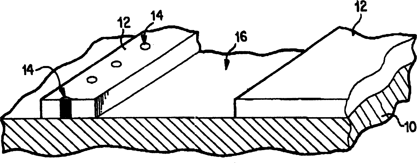
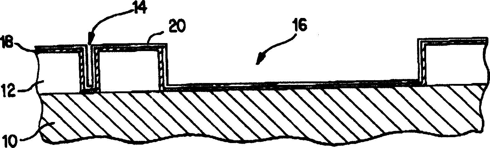
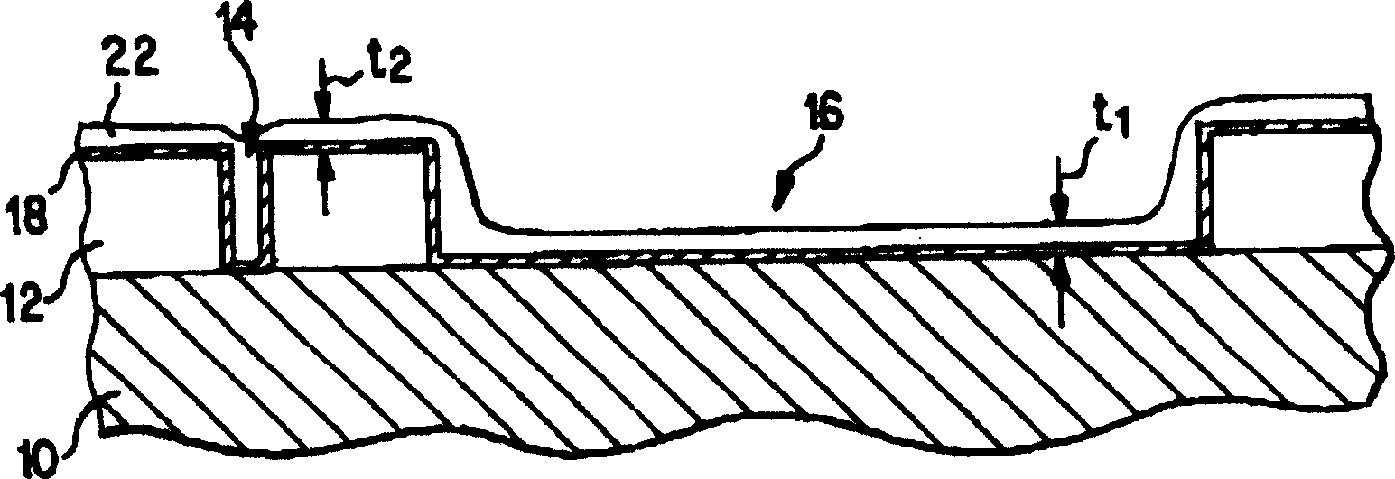
[0049] The present invention provides a method and system for controlling the uniformity of deposition of a layer of conductive material on a semiconductor surface. The invention can be used with ECMD, masked pulse plating, and full surface plating, as well as plating systems that deposit conformal coatings. The deposition process of the present invention advantageously accomplishes the deposition of plating material in numerous cavities, such as trenches, holes, contact holes and the like, on the surface of a semiconductor wafer.

[0050] As is known, during electrodeposition of a wafer surface, the current density applied to the surface is much stronger at the periphery of the surface than in the middle of the surface. In the prior art, this higher current density results in a higher deposition rate of the deposited coating at the periphery of the wafer compared to the center of the wafer. During electrodeposition, using the combination of the perforated plate or a mask and...


PUM


Abstract

An apparatus which can control thickness uniformity during deposition of conductive material from an electrolyte onto a surface of a semiconductor substrate is provided. The apparatus has an anode which can be contacted by the electrolyte during deposition of the conductive material, a cathode assembly including a carrier adapted to carry the substrate for movement during deposition, and a conductive element permitting electrolyte flow therethrough. A mask lies over the conductive element and has openings permitting electrolyte flow. The openings define active regions of the conductive element by which a rate of conductive material deposition onto the surface can be varied. A power source can provide a potential between the anode and the cathode assembly so as to produce the deposition. A deposition process is also disclosed, and uniform electroetching of conductive material on the semiconductor substrate surface can additionally be performed.

Description

technical field [0001] This invention relates to electrodeposition processing technology, and more particularly to electrodeposition processing and apparatus for producing planar deposited layers. Background technique [0002] Conventional semiconductor devices generally include a semiconductor substrate, usually a silicon substrate; several successively formed dielectric layers, such as silicon dioxide layers; and conductive lines or interconnections made of conductive substances. Interconnects are typically formed by filling conductive substances into trenches etched into a dielectric layer. In integrated circuits, multi-layered interconnections extend laterally across the surface of the substrate. Interconnects formed at different levels are electrically connected using vias and contacts. Filling of such components with a conductive substance, ie via openings, slots, pads or contacts, can be carried out by depositing a conductive substan...

Claims


Application Information

Patent Timeline
Patent Type & Authority Applications(China)
IPC IPC(8): C25D17/00C25D7/12C25D17/10C25D21/00C25D21/12C25F7/00H01L21/288H01L21/768
CPCC25D7/12H01L21/76877C25D7/123H01L21/2885Y10S204/07C25D17/001C25F7/00C25D17/00
Inventor 布伦特·M·贝斯保罗·林德奎斯特
Owner 纽仪器股份有限公司
Why Eureka
Try Eureka