

Liquid crystal display panel
A liquid crystal display panel, liquid crystal technology, applied in nonlinear optics, instruments, optics, etc., can solve problems such as poor filling
- Summary
- Abstract
- Description
- Claims
- Application Information
AI Technical Summary
Problems solved by technology
Method used
Image

Examples
no. 1 approach
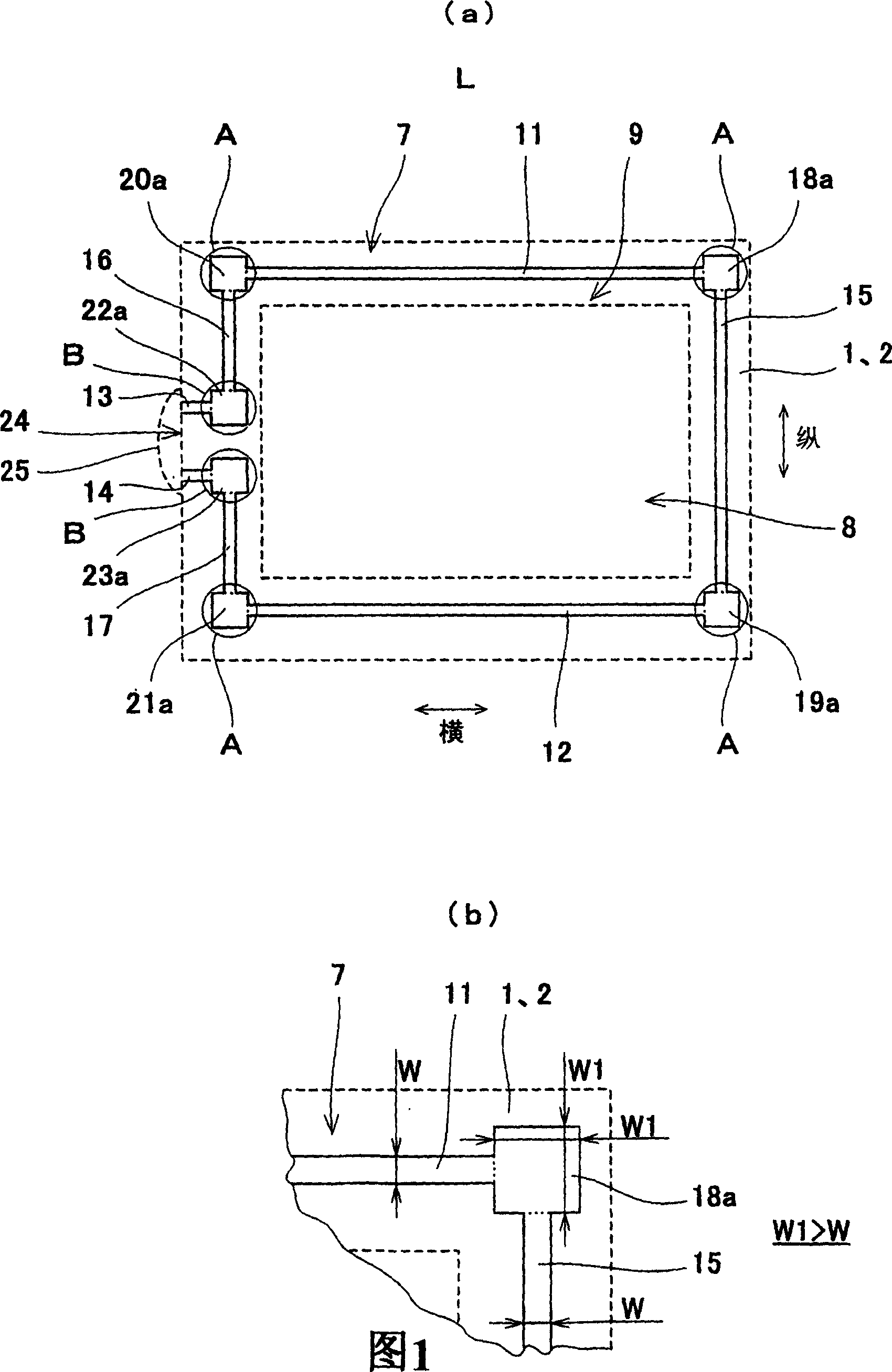
[0029] The first embodiment of the present invention shows a first configuration example of a liquid crystal display panel in which the outflow of a liquid crystal material can be prevented by making the pattern width of the corner pattern wider than that of other patterns other than the corner pattern.
[0030] 1( a ) and FIG. 1( b ) are diagrams schematically showing the shape of a seal pattern for liquid crystal sealing according to the first embodiment of the present invention. Overall plan view of the pattern; FIG. 1( b ) is a plan view enlargedly showing a corner pattern of the seal pattern for liquid crystal sealing in FIG. 1( a ). Here, for convenience of description, the direction of the seal pattern for liquid crystal sealing is shown as shown in the figure. In addition, in Figure 1 with Figure 7 The same reference numerals denote the same or corresponding parts.
[0031] The seal pattern 7 for liquid crystal sealing arranged on the liquid crystal display panel L ...
no. 2 approach
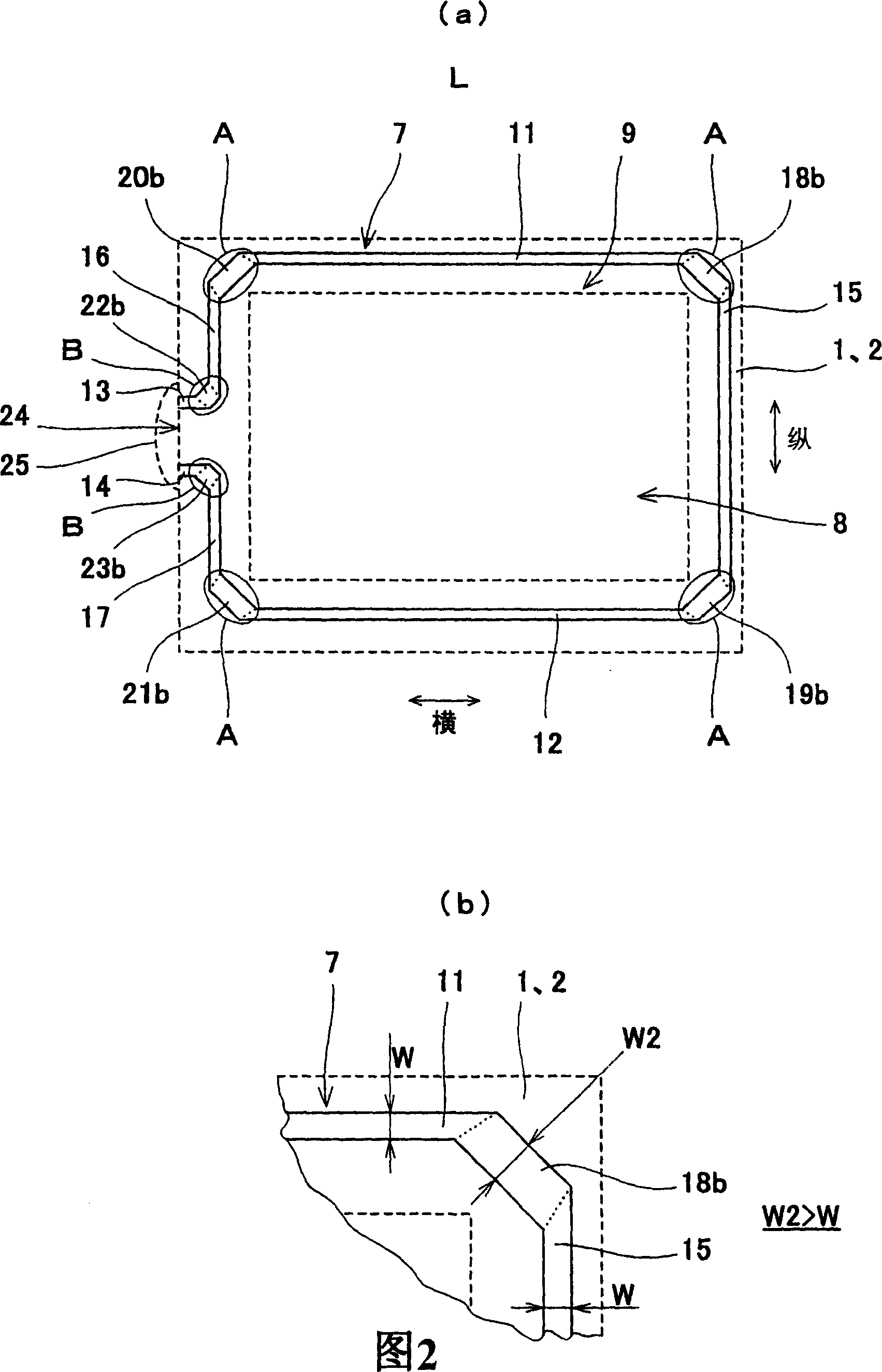
[0039] The second embodiment of the present invention shows a second structural example of a liquid crystal display panel in which the outflow of a liquid crystal material can be prevented by forming the image width of the corner pattern wider than that of other patterns other than the corner pattern.
[0040] Fig. 2 (a) and Fig. 2 (b) are the figures that schematically show the shape of the seal pattern for liquid crystal sealing of the second embodiment of the present invention; The plan view of the whole pattern; FIG. 2( b ) is a plan view enlargedly showing the corner pattern of the seal pattern for liquid crystal sealing in FIG. 2( a ). In addition, in Figure 2 with Figure 7 The same reference numerals denote the same or corresponding parts.
[0041] As shown in FIG. 2(a) and FIG. 2(b), in this embodiment, the pattern width W2 of the corner patterns 18b to 21b and 22b to 23b of the seal pattern 7 for liquid crystal sealing is formed to be wider than that of the corner p...
no. 3 approach
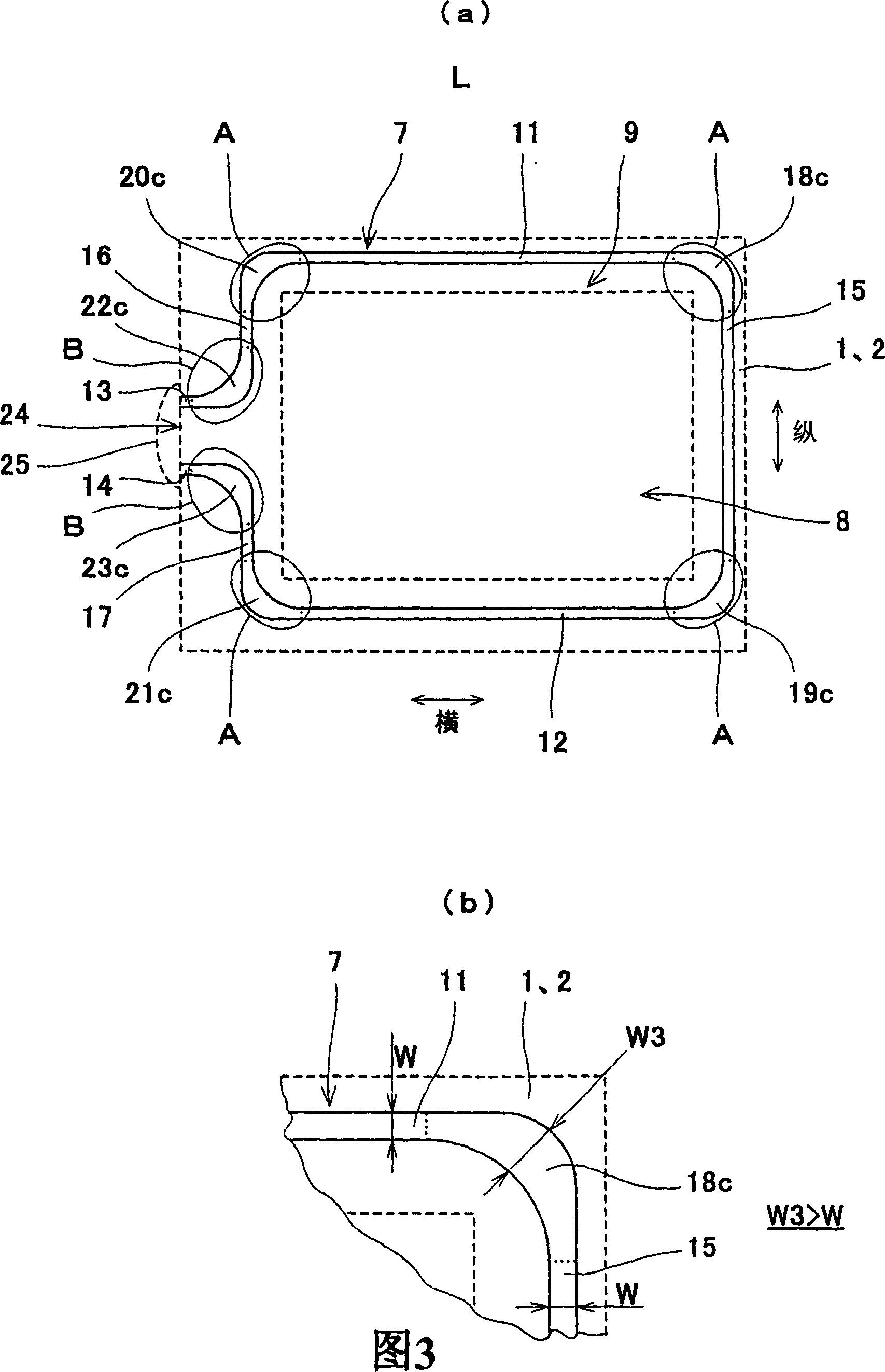
[0045] The third embodiment of the present invention shows a third structural example of a liquid crystal display panel in which the outflow of a liquid crystal material can be prevented by forming the pattern width of the corner pattern wider than that of other patterns other than the corner pattern.
[0046] Fig. 3 (a) and Fig. 3 (b) are the figures that schematically show the shape of the seal pattern for liquid crystal sealing of the third embodiment of the present invention; The plan view of the whole pattern; FIG. 3( b ) is a plan view enlargedly showing the corner pattern of the seal pattern for liquid crystal sealing in FIG. 3( a ). In addition, in Figure 3 with Figure 7 The same reference numerals denote the same or corresponding parts.
[0047] As shown in FIG. 3( a ) and FIG. 3( b ), in this embodiment, the corner patterns 18c to 21c and 22c to 23c of the seal pattern 7 for liquid crystal sealing are formed such that the pattern width W3 at the center is connected...
PUM
 Abstract
Description
Claims
Application Information