

Film transistor LCD and method for manufacturing same
A technology of thin-film transistors and liquid crystal displays, applied in transistors, instruments, optics, etc., can solve problems such as difficulties, achieve the effect of simplifying the process and increasing the pixel aperture ratio
- Summary
- Abstract
- Description
- Claims
- Application Information
AI Technical Summary
Problems solved by technology
Method used
Image

Examples
no. 1 example
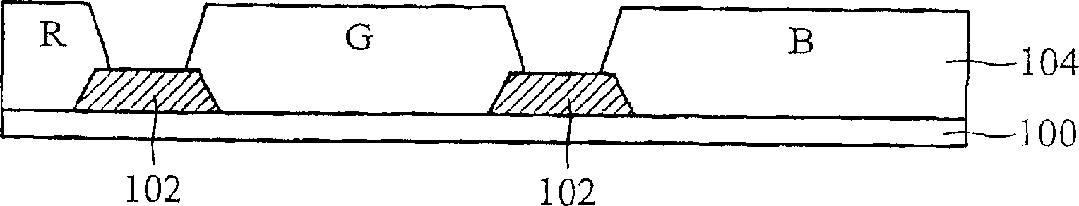
[0088] Figure 2A to Figure 2G A schematic cross-sectional view showing a method of forming a TOC substrate of a liquid crystal display according to a first embodiment of the present invention.
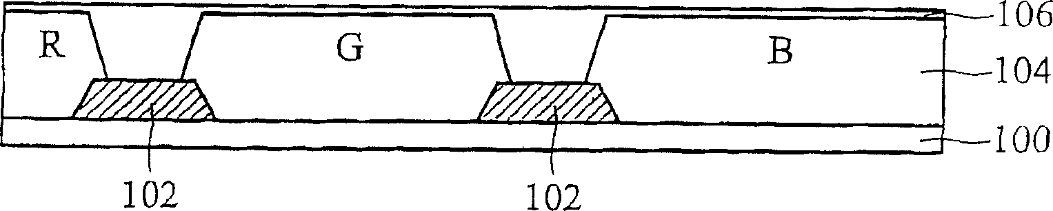
[0089] Please refer to Figure 2A Firstly, a substrate 100 is provided, and its material is a transparent insulating material, such as glass. Afterwards, a data line 102 is formed on the substrate 100 , and the data line is defined by the first metal layer ( M1 ), which is also used for light shielding. The data line 102 may be alloys of Al, Cr, Mo, Ta, Ti, Cu or combinations thereof. The color filter layer 104 is formed on the data line 102 and the substrate 100 , wherein the color filter layer 104 includes three main colors: red (R), blue (B) and green (G), and respectively correspond to pixel regions.
[0090] Then please refer to Figure 2B , the data line 102 and the color filter layer 104 are covered by a covering layer 106, which is made of a high-temperature-resistant orga...
no. 2 example
[0098] Figure 3A to Figure 3G A schematic cross-sectional view showing a method for forming a TOC substrate of a liquid crystal display according to a second embodiment of the present invention.
[0099] Please refer to Figure 3A Firstly, a substrate 200 is provided, and its material is a transparent insulating material, such as glass. Afterwards, a data line 202 is formed on the substrate 200, and the data line is defined and formed by the first metal layer (M1), which is also used for light shielding. The data line 202 may be alloys of Al, Cr, Mo, Ta, Ti, Cu or combinations thereof. The color filter layer 204 is formed on the data line 202 and the substrate 200 , wherein the color filter layer 204 includes three main colors: red (R), blue (B) and green (G), respectively corresponding to the pixel areas.
[0100] Then please refer to Figure 3B , the data lines 202 and the color filter layer 204 are covered by a covering layer 206, which is made of photosensitive or non...
no. 3 example
[0107] Figure 4A to Figure 4G A schematic cross-sectional view showing a method for forming a TOC substrate of a liquid crystal display according to a third embodiment of the present invention.
[0108] Please refer to Figure 4A Firstly, a substrate 300 is provided, and its material is a transparent insulating material, such as glass. Afterwards, a data line 302 is formed on the substrate 300, and the data line is defined and formed by the first metal layer (M1), which is also used for light shielding. The data line 302 may be alloys of Al, Cr, Mo, Ta, Ti, Cu or combinations thereof. The color filter layer 304 is formed on the data line 302 and the substrate 300 , wherein the color filter layer 304 includes three main colors: red (R), blue (B) and green (G), respectively corresponding to the pixel areas.
[0109] Then please refer to Figure 4B , the data lines 302 and the color filter layer 304 are covered by a covering layer 306, the material of which can be photosensi...
PUM
 Abstract
Description
Claims
Application Information