Semiconductor memory device and semiconductor integrated circuit device

A storage device and semiconductor technology, applied in the direction of information storage, static memory, digital memory information, etc., can solve the problems of increased power consumption, inability to maintain data, frequent refresh operations, etc., and achieve the optimization of operation time and simplification of refresh control Effect

Inactive Publication Date: 2005-02-02
PANASONIC CORP
View PDF3 Cites 15 Cited by
  • Summary
  • Abstract
  • Description
  • Claims
  • Application Information

AI Technical Summary

Problems solved by technology

However, the read and write action requests are continuous, and the number of NOP cycles is very small. Since a given number of refresh actions must be performed every certain cycle, if the required number of times is not reached, the data will not be maintained.
[0009] In the DRAM of Patent Document 3, even if the refresh operation is not performed from the outside, the data of the memory cell can be retained by an internal refresh operation inserted before the processing of the read and write operations, and even if the read and write access request does not carry a NOP Refresh operations can be performed accurately even in continuous situations, but if frequent read and write operations are performed, refresh operations will also become frequent, so power consumption will increase

Method used


Image

  • Semiconductor memory device and semiconductor integrated circuit device
  • Semiconductor memory device and semiconductor integrated circuit device
  • Semiconductor memory device and semiconductor integrated circuit device

Examples


no. 1 approach

[0045] -Overall composition-

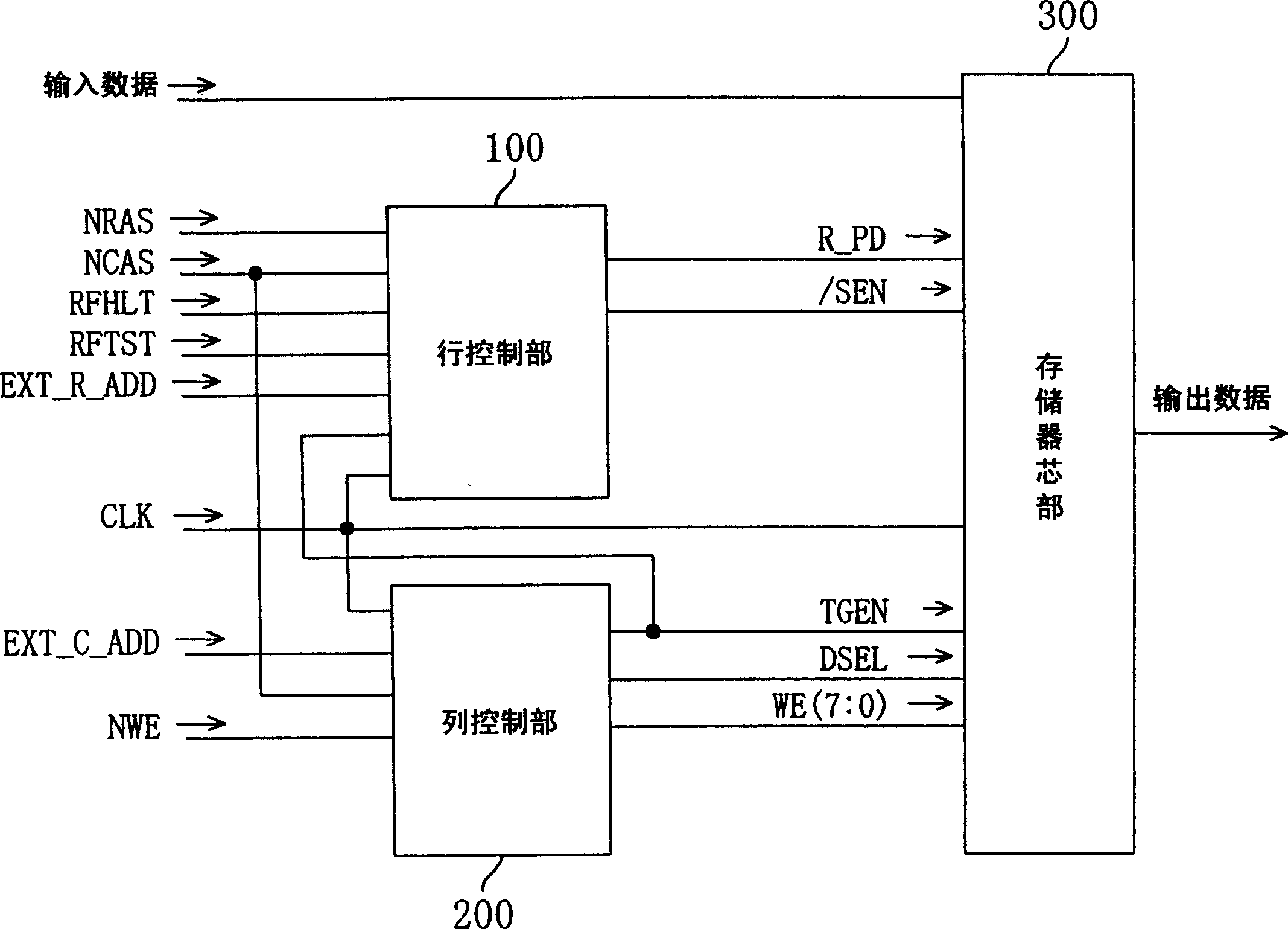
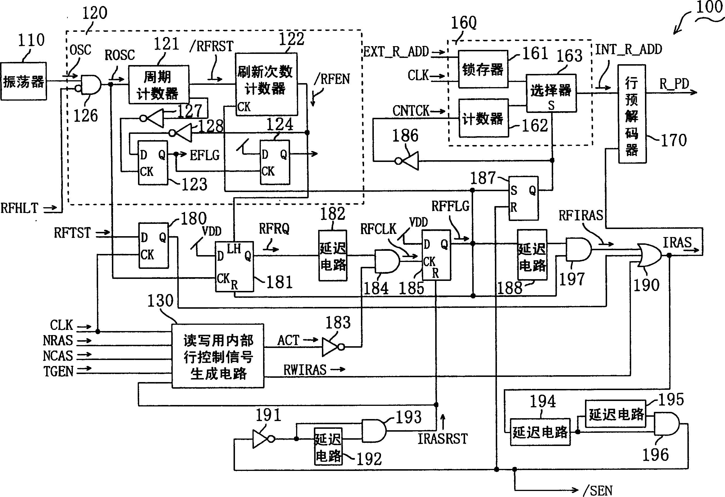
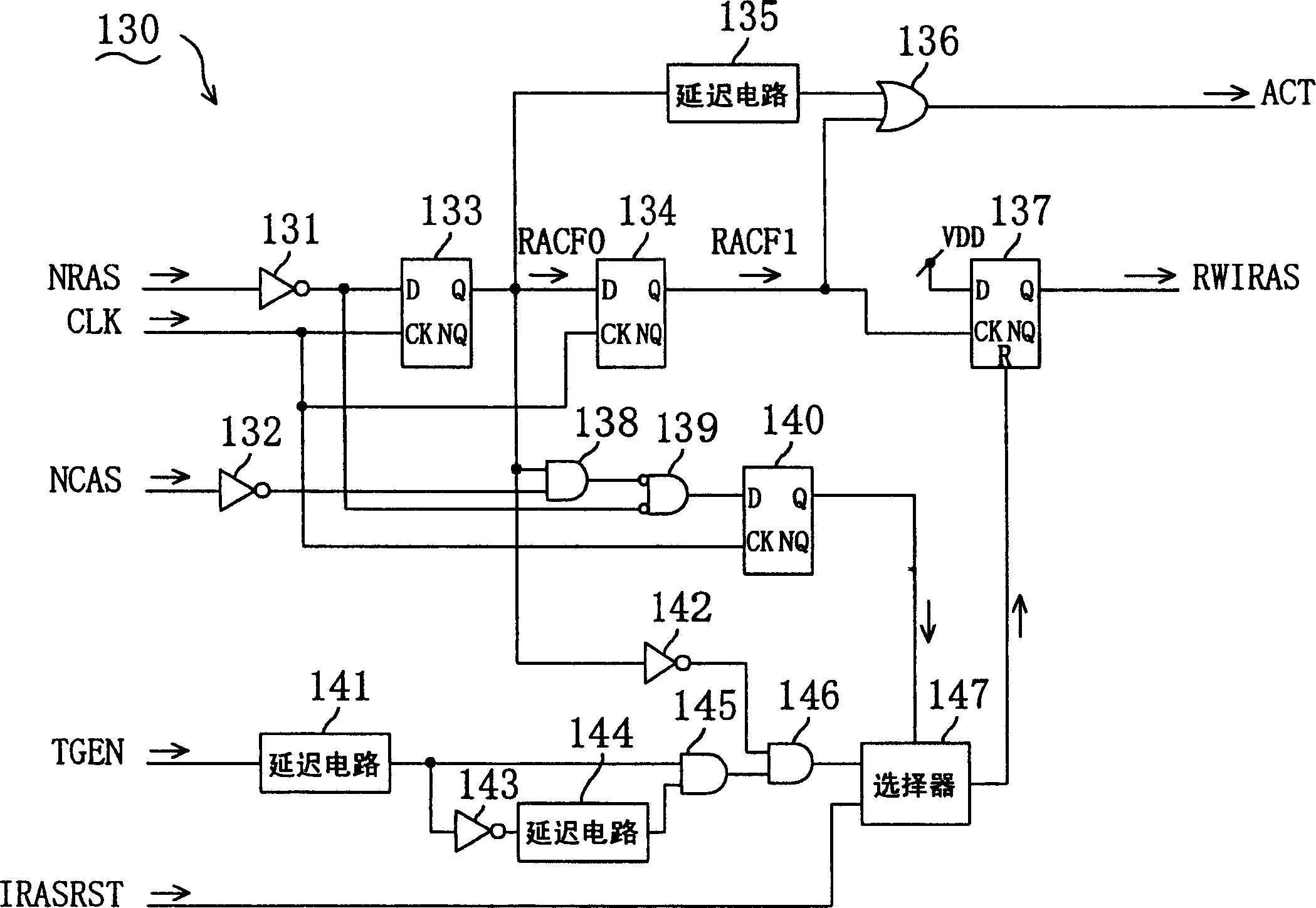
[0046] figure 1 A schematic circuit block diagram showing the structure of the semiconductor memory device according to the first embodiment. As shown in the figure, the semiconductor memory device of this embodiment includes: a memory cell array having memory cells arranged in rows and columns; word lines extending along the row direction of the memory cell array; word lines extending along the column direction of the memory cell array; A memory core 300 such as a bit line for amplifying a signal read from a memory cell, a sense amplifier, etc.; a row control circuit 100 for controlling selection and non-selection of a word line; and a column for controlling selection and non-selection of a bit line, etc. Control circuit 200.

[0047] The row control circuit 100 receives a row control signal NRSA, a column control signal NCAS, a refresh stop signal RFHLT, a test refresh signal RFTST, an external row address EXT_R_ADD, and an external clock CL...

no. 2 approach

[0088] Figure 7 A schematic configuration diagram showing a semiconductor integrated circuit device according to a second embodiment of the present invention. As shown in the figure, the semiconductor integrated circuit device of this embodiment includes: a logic unit 400 composed of a CMOS device including a CPU or various arithmetic circuits; and a memory unit 500 (DRAM) which is figure 1 The semiconductor memory device shown. exist Image 6 In the shown semiconductor integrated circuit device, the structure of the memory unit 500 is the same as that in the first embodiment Figure 1 ~ Figure 4 Same as shown. A CPU, a plurality of arithmetic circuits, and the like are arranged in the logic unit 400 .

[0089] Then, a row control signal NRAS, a column control signal NCAS, a read enable NWE, an external row address EXT_R_ADD, an external column address EXT_C_ADD, input data, and the like are transferred from the logic section 400 to the memory section 500 . These signal...


PUM


Abstract

A row control circuit 100 of the semiconductor memory device is provided with an oscillator 110 as a clock oscillator for generating an internal clock, a D flipflop 181 as a refresh request signal RFRQ generation circuit for generating a refresh request signal RFRQ synchronously with the internal clock and a delay circuit 182, a NAND gate 184, an AND gate 182, a D flipflop 185, a delay circuit 188, an AND gate 189 and an OR gate 190 as refresh control circuits. By using a refresh request signal RFRQ and an active signal ACT, internal refresh is performed internally in a DRAM separately from an external refresh command. To provide a semiconductor memory device and a semiconductor integrated circuit device capable of simplifying the memory control while securing the sufficient refresh function.

Description

technical field [0001] The present invention relates to a semiconductor memory device and a semiconductor integrated circuit device including memory cells that need to be refreshed in order to hold data. Background technique [0002] DRAM requires a refresh operation in order to retain data in memory cells. In the DRAM disclosed in Patent Document 1, an auto-refresh operation of refreshing by an external refresh request signal and a self-refresh operation of refreshing by an internal timer by setting the DRAM to a self-refresh mode can be realized. [0003] In the case of automatic refresh, a refresh request signal must be generated externally and provided to the DRAM during the interval between read and write operations, so as to perform a given number of refresh operations at regular intervals. [0004] In the case of self-refresh, since the refresh operation of DRAM is started according to the internal timer, there is no need to generate timing signals for each refresh o...

Claims


Application Information

Patent Timeline
Patent Type & Authority Applications(China)
IPC IPC(8): G11C11/406
CPCG11C2211/4061G11C11/406G11C11/40615
Inventor 藤本知则大田清人菊川博仁
Owner PANASONIC CORP
Why Eureka
Try Eureka