Supercharge Your Innovation With Domain-Expert AI Agents!

Semiconductor design layout pattern formation method and graphic pattern formation unit

A semiconductor and layout technology, used in semiconductor/solid-state device manufacturing, computer-aided design, CAD circuit design, etc., to solve problems such as insufficient correction accuracy

Inactive Publication Date: 2005-02-02
PANASONIC CORP
View PDF0 Cites 3 Cited by
  • Summary
  • Abstract
  • Description
  • Claims
  • Application Information

AI Technical Summary

Problems solved by technology

[0006] However, unless the receding amount of one end portion is estimated for each combination of an edge portion of a line pattern and a peripheral pattern, thereby setting a correction amount for the value, according to the above-mentioned mask pattern correction method according to the prior art Inability to achieve sufficient correction accuracy

Method used


Image

  • Semiconductor design layout pattern formation method and graphic pattern formation unit
  • Semiconductor design layout pattern formation method and graphic pattern formation unit
  • Semiconductor design layout pattern formation method and graphic pattern formation unit

Examples


Embodiment Construction

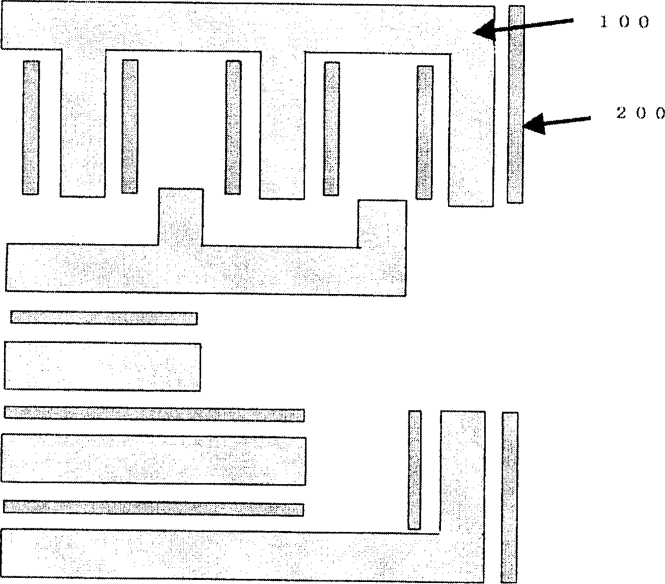
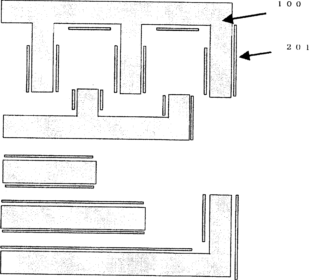
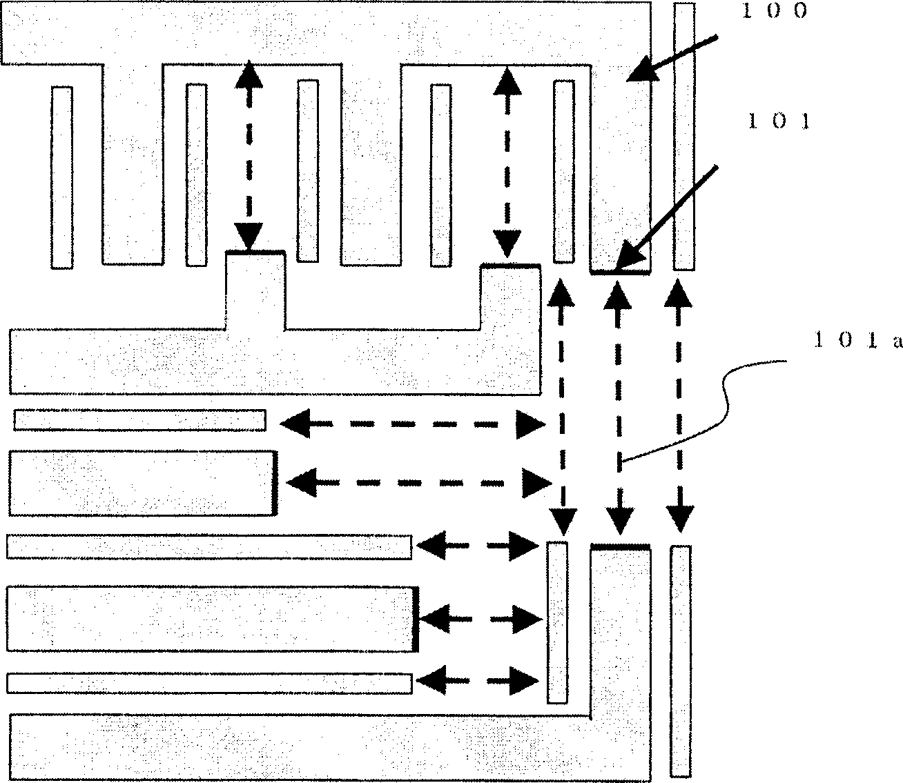
[0048] Refer to the following figure 1 A first embodiment of the present invention is described. figure 1 It is a layout plan view after forming a virtual graphic pattern according to the semiconductor design layout forming method of the first embodiment of the present invention.

[0049] exist figure 1 In , the entire layout is denoted as 100, and a dummy pattern is denoted as 200. Such as figure 1 As shown, in order to make the effect of each line end on the wafer uniform, a dummy graphic pattern 200 that has nothing to do with other wiring is placed between each wiring (non-wiring area), so that the wiring design is not included in the design layout 100. In the case of having the same pitch, make the wiring have the same pitch. That is, this pattern forming method includes the step of forming the above-mentioned dummy graphic pattern 200 , which is set so that the interval between the dummy graphic pattern 200 and the wiring becomes the same. Thereby, the receding ...


PUM


Abstract

Reduction in labor of the operations for evaluating the amount of retrogression of end portions in a line pattern, and the simplification of the CAD processing for a mask are achieved. A semiconductor design layout pattern formation method is provided concerning a layout pattern on a wafer, wherein the designed wire lines do not have the same pitch, and wherein a dummy graphic pattern having no relation to wiring is formed in a non-wired region of the layout pattern so that the interval between the dummy graphic pattern and the adjacent wiring line becomes equal to the intervals of wiring lines. It becomes possible to make uniform the pitch of the end portions of lines in the design layout pattern on the wafer, so that the dispersion in the change of the form (retrogression) of the end portions of the lines can be restricted. Thereby, the amount of retrogression on the wafer can be made uniform, so that the specification of the formation of hammer graphics can be simplified, and it becomes possible to reduce the time period necessary for mask CAD processing, and also to reduce the amount of mask data.

Description

technical field [0001] The present invention relates to a photomask data processing technique for compensating pattern degradation during wafer processing for semiconductor manufacturing. In addition, the present invention relates to a semiconductor design layout forming method and a graphic pattern forming unit related to photomask data. Background technique [0002] Since the ends of the lines of the semiconductor design layout are significantly recessed on the wafer, an auxiliary pattern called a hammer (or serif) pattern needs to be added to the mask data Each end of each line to prevent pattern changes on the wafer. [0003] Typically, the amount of retrogression at each end of each line in the layout on the wafer is estimated by experimentation, and a hammer pattern having a certain size and shape is added to each end of each line. For example, if Figure 18 As shown, measure the line width 1 of the layout 0; according to the edge length 2 between the ends of the lin...

Claims


Application Information

Patent Timeline
IPC IPC(8): G03F1/68G03F1/70G03F7/20G06F17/50H01L21/027
CPCG06F17/5068G06F30/39
Inventor 山际实谷本正三坂章夫日野上丽子
Owner PANASONIC CORP
Features
  • R&D
  • Intellectual Property
  • Life Sciences
  • Materials
  • Tech Scout
  • Unparalleled Data Quality
  • Higher Quality Content
  • 60% Fewer Hallucinations
Learn More