Lsi package

A technology of power path and multi-layer circuit board, which is applied in the direction of circuits, printed circuits, printed circuits connected with non-printed electrical components, etc. Effects of Electromagnetic Radiation

Inactive Publication Date: 2005-02-02
PANASONIC CORP
View PDF0 Cites 9 Cited by
  • Summary
  • Abstract
  • Description
  • Claims
  • Application Information

AI Technical Summary

Problems solved by technology

Therefore, the power supply terminal on the LSI chip is not supplied with a high enough voltage

Method used


Image

  • Lsi package
  • Lsi package
  • Lsi package

Examples


Embodiment Construction

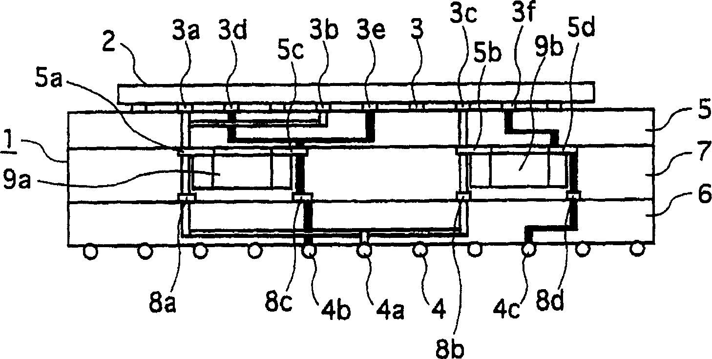
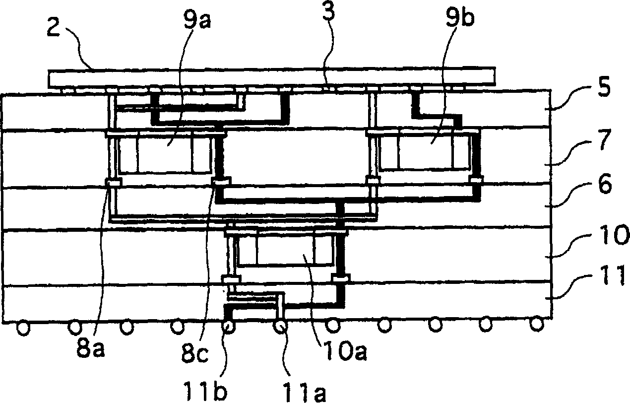
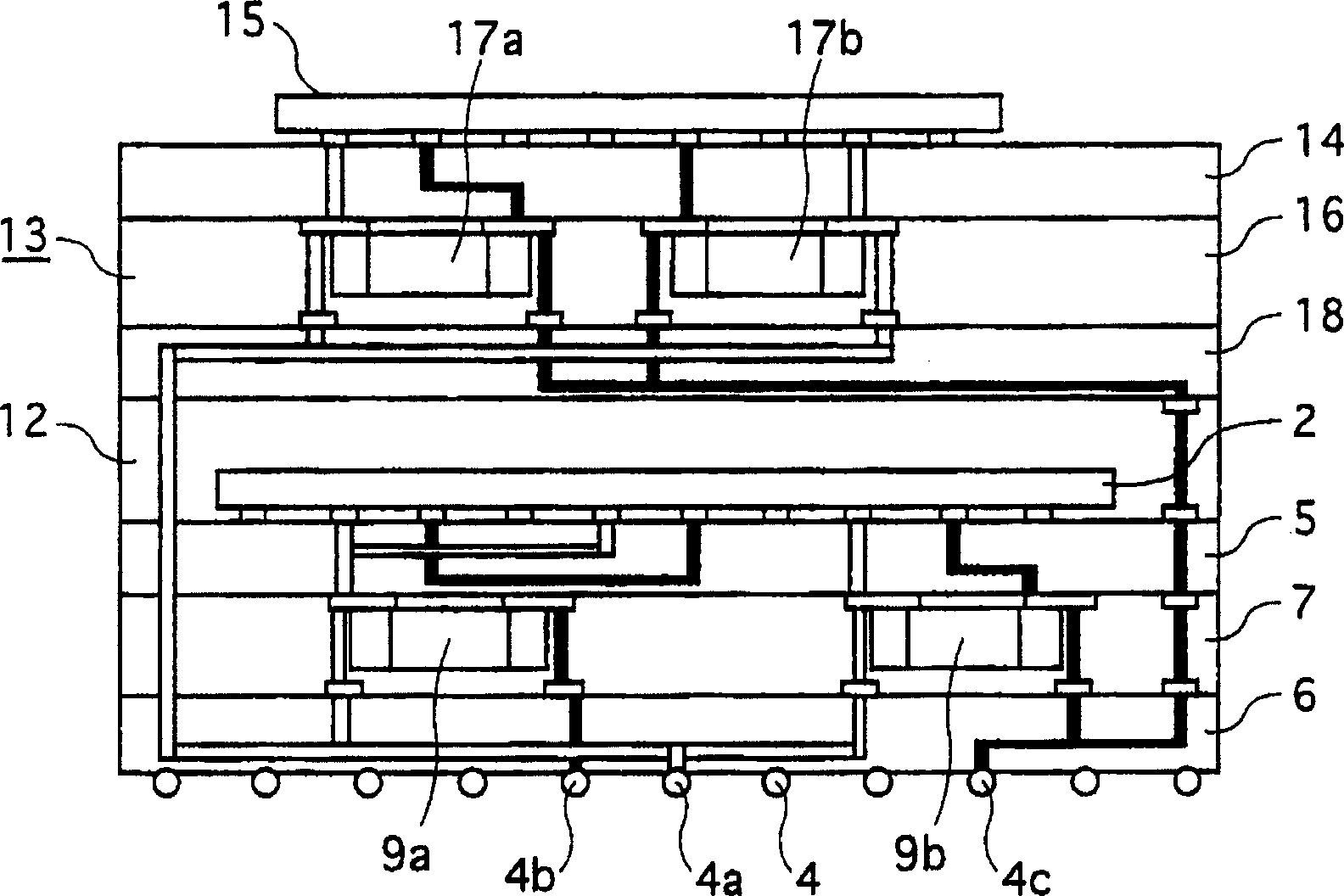
[0040] The following part explains the LSI package related to the embodiment of the present invention with reference to the drawings. The drawing shows a cross-sectional view of an LSI package, and hatching is not included for better understanding of the structure.

[0041] Such as figure 1 As shown in , an LSI package includes a substrate 1 and an LSI chip 2 forming a main body of the LSI package. A plurality of bumps are arranged in a grid pattern on the LSI chip 2 as terminals 3 . A plurality of solder balls are arranged in a grid pattern on one surface of the substrate 1 as terminals 4 . Terminals 3 and 4 include signal input / output terminals, power supply terminals and ground terminals. Since the signal input / output terminal is not directly related to the present invention, it is not explained here.

[0042] The substrate 1 has a three-layer structure including a multilayer circuit board 6 on which a terminal 4 is provided, a multilayer circuit board 5 on which an LSI...


PUM


Abstract

According to LSI packages of the BGA type and the like, the number of source voltage supply terminals on an LSI package needs to be around the same as the number of power supply terminals on an LSI chip, in order to prevent the impact of high-frequency currents generated due to a switching operation in an internal circuit in the LSI chip. According to the present invention, however, at least two power supply terminals on an LSI chip are connected to one source voltage supply terminal on an LSI package. In addition, a capacitor element is embedded in a substrate forming the main body of the LSI package, and the capacitor element is provided between a source voltage supply terminal and an earth terminal.

Description

technical field [0001] The invention relates to a large scale integrated circuit (LSI) packaging technology. Background technique [0002] Recently, the number of pins in LSIs has been increasing in accordance with the demand for more complex LSIs. On the other hand, miniaturized packages for LSIs are expected in accordance with demands for miniaturized devices and boards. For this reason, a ball grid array (BGA) type and a chip size package (CSP) shown in FIGS. 9A and 9B replace the quad flat package (QFP) shown in FIGS. 8A and 8B . According to the CSP type, the size of the LSI package is substantially the same as that of the LSI chip. According to the BGA and CSP LSI package technologies, terminals (solder balls) connected to printed wiring board wiring are arranged in a grid pattern on the back surface of the LSI package. [0003] In LSI packages of BGA and CSP, solder balls located near the periphery are connected by wires to wirings formed on the mounting surface of...

Claims


Application Information

Patent Timeline
Patent Type & Authority Applications(China)
IPC IPC(8): H01L25/00H01L23/498H01L23/50H01L23/538H05K1/18
CPCH01L2924/15311H01L23/50H01L23/49822H01L2224/16225H01L2924/3025H05K1/185H01L2224/16H01L23/5389H01L2224/05573H01L2224/05568H01L2924/00014H01L2224/05599
Inventor 末永宽齐藤义行
Owner PANASONIC CORP
Why Eureka
Try Eureka