

Photoelectric device and its manufacture, substrate cutting method and substrates for photoelectric devices
An electro-optic device and manufacturing method technology, applied to identification devices, manufacturing tools, glass manufacturing equipment, etc., can solve problems such as manual segmentation, defects, and increased costs
- Summary
- Abstract
- Description
- Claims
- Application Information
AI Technical Summary
Problems solved by technology
Method used
Image

Examples
Embodiment Construction
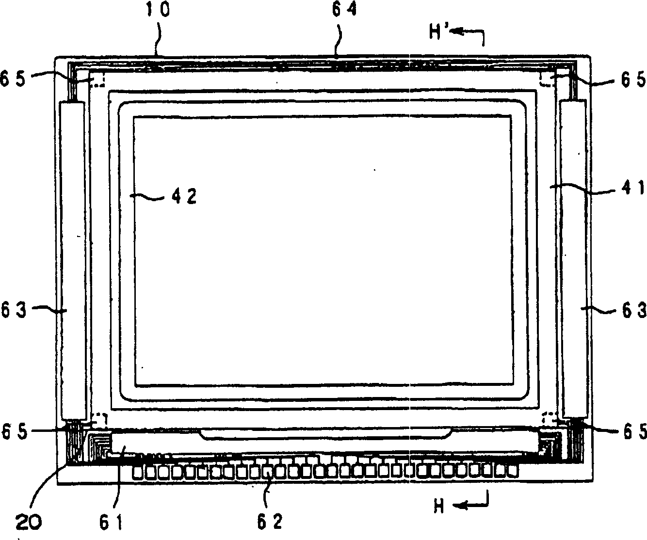
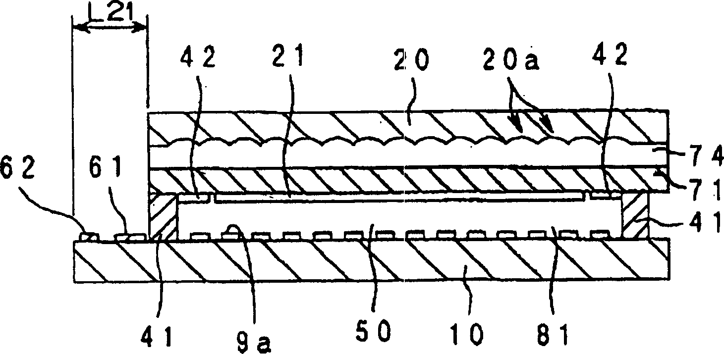
[0084] Hereinafter, embodiments of the present invention will be described in detail with reference to the drawings. figure 1 It is a plan view of a liquid crystal display device according to an embodiment of the present invention. This embodiment is applied to a TFT liquid crystal display device as one of electro-optic devices, figure 1 This is a view of an element substrate such as a TFT substrate and components formed thereon viewed from the counter substrate side. figure 2 is in figure 1 The position of the H-H' line in the figure is a cross-sectional view of the liquid crystal display device after the assembly process is cut.
[0085] Such as figure 1 and figure 2 As shown, a liquid crystal display device such as a liquid crystal panel is configured by sealing a liquid crystal 50 between an element 10 such as a TFT substrate and a counter substrate 20 . In '10, (ITO)9a etc. are arranged in matrix. In addition, an upper cover glass 71 is attached to the counter s...
PUM
 Abstract
Description
Claims
Application Information