Trench mosfet having low gate charge

A trench and trench sidewall technology, applied in the field of trench MOSFET devices, can solve problems such as gate charge increase, and achieve the effect of reducing the state charge level

Inactive Publication Date: 2005-02-23
GEN SEMICON
View PDF2 Cites 10 Cited by
  • Summary
  • Abstract
  • Description
  • Claims
  • Application Information

AI Technical Summary

Problems solved by technology

Unfortunately, as component density increases, the gate charge associated with trench MOSFET devices increases

Method used


Image

  • Trench mosfet having low gate charge
  • Trench mosfet having low gate charge
  • Trench mosfet having low gate charge

Examples


Embodiment Construction

[0035] Hereinafter, the present invention will be fully described with reference to the accompanying drawings, which show preferred embodiments of the invention. Furthermore, the invention may be embodied in different forms and should not be construed as limited to the embodiments described herein.

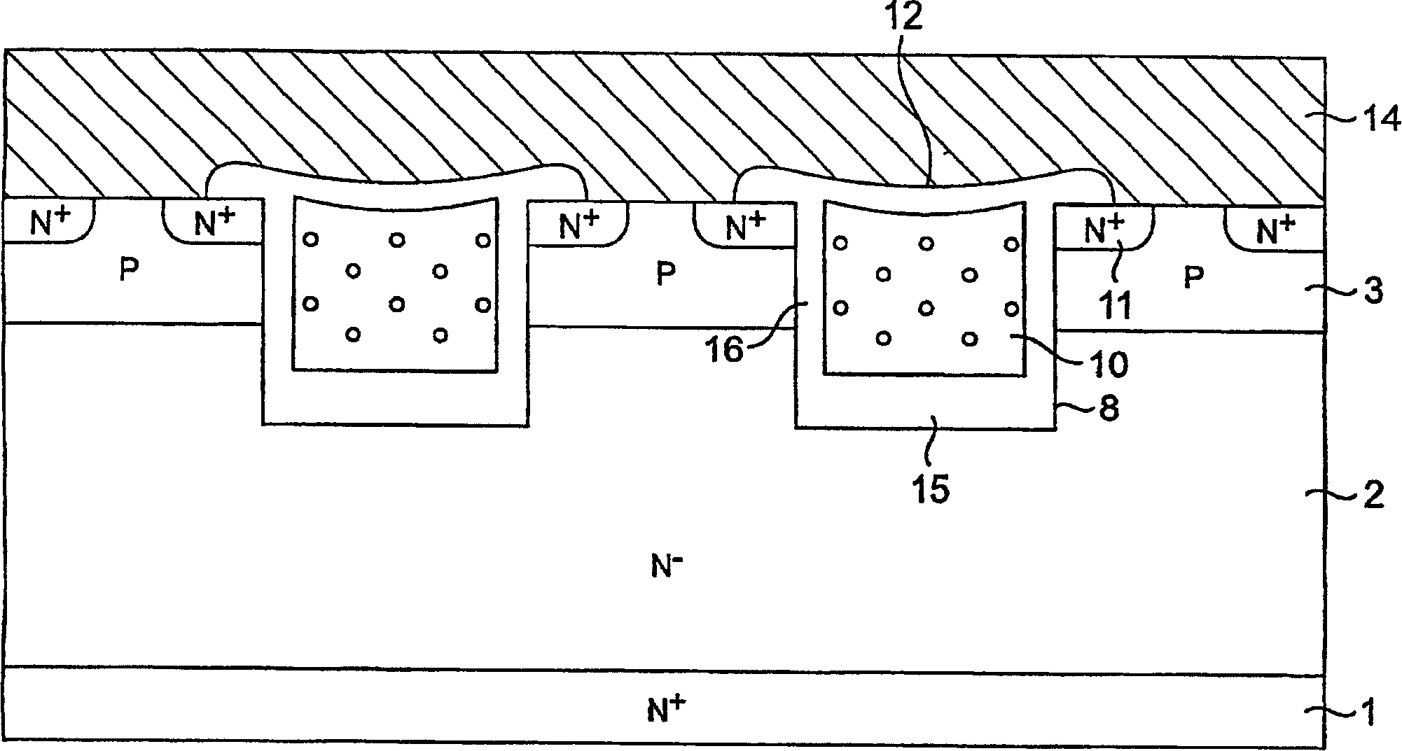
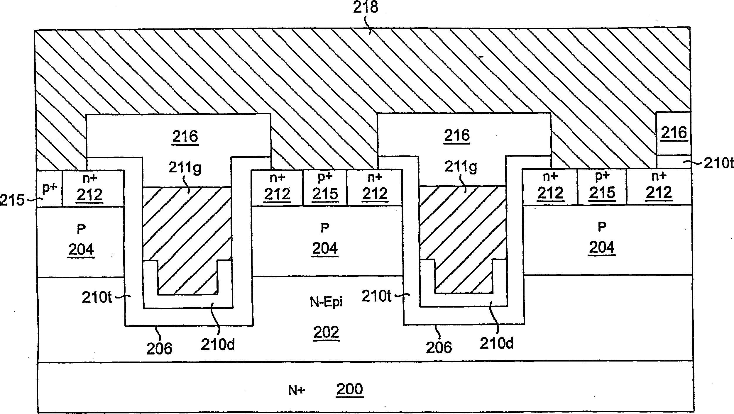
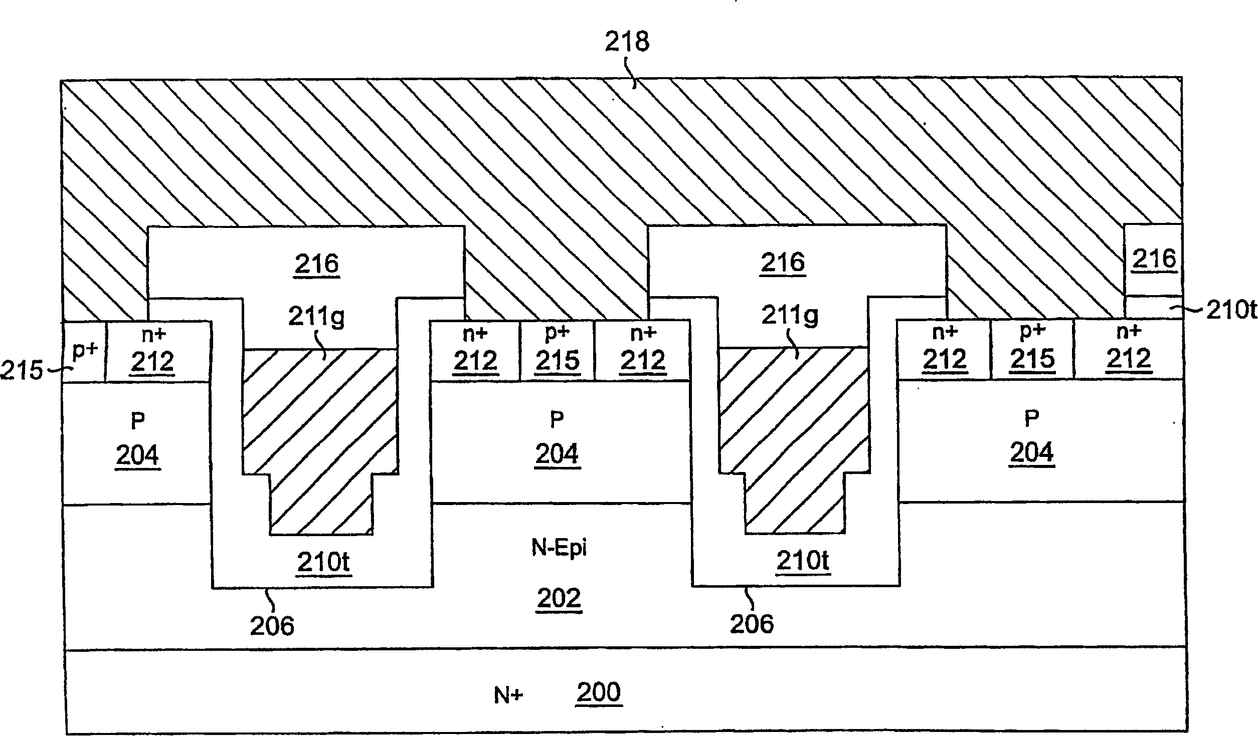
[0036] exist figure 2 One embodiment of the trench MOSFET of the present invention is shown in partial cross-section in . The illustrated trench MOSFET includes an N-type epitaxial layer 202 disposed on an N+ substrate 200 . N+ substrate 200 is typically a silicon substrate having a thickness ranging, for example, from 10 to 25 mils (mil), and a resistivity ranging, for example, from 0.005 Ohm-cm to 0.01 Ohm-cm . N-type epitaxial layer 202 is also typically silicon, having a thickness ranging, eg, from 5 microns to 6 microns, and a resistivity ranging, eg, from 0.18 Ohm-cm to 0.25 Ohm-cm.

[0037] A trench 206 formed in the epitaxial layer is lined with a thermally grown oxide...


PUM


Abstract

A trench MOSFET device comprising: (a) a silicon substrate (200) of a first conductivity type (preferably N-type conductivity); (b) a silicon epitaxial layer (202) of the first conductivity type over the substrate, the epitaxial layer having a lower majority carrier concentration than the substrate; (c) a body region (204) of a second conductivity type (preferably P-type conductivity) within an upper portion of the epitaxial layer; (d) a trench (206) having trench sidewalls and a trench bottom, which extends into the epitaxial layer from an upper surface of the epitaxial layer and through the body region of the device; (f) an oxide region (210t) lining the trench, which comprises a lower segment (210d) covering at least the trench bottom and upper segments covering at least upper regions of the trench sidewalls; (g) a conductive region (211g) within the trench adjacent the oxide region; and (h) a source region (212) of the first conductivity type within an upper portion of the body region and adjacent the trench. The lower segment (210d) of the oxide region is thicker than the upper segments of the oxide region in this embodiment.

Description

technical field [0001] The present invention relates to microelectronic circuits, and more particularly to trench MOSFET devices with low gate charge. Background technique [0002] Metal Oxide Semiconductor Field Effect Transistor (MOSFET) devices utilizing trench gates provide low on-resistance. In such trench MOSFET devices, the channels are arranged vertically instead of horizontally as in most planar structures. Such transistors provide high current per unit area where low forward voltage drop is required. [0003] FIG. 1 shows a partial cross-sectional view of a trench MOSFET device comprising an N+ substrate 1 , an N− epitaxial layer 2 , a P body region 3 and an N+ region 11 . Typically, the P body region 3 is diffused into the N − epitaxial layer 2 arranged on the N+ substrate 1 , while the N+ region 11 is in turn diffused in the body region 3 . Due to the application of two diffusion steps, this type of transistor is often referred to as a double-diffused metal-ox...

Claims


Application Information

Patent Timeline
Patent Type & Authority Applications(China)
IPC IPC(8): H01L21/28H01L21/336H01L29/423H01L29/51H01L29/78
CPCH01L29/4925H01L29/7813H01L21/28185H01L29/42368H01L29/513H01L29/4933H01L29/511H01L21/28194
Inventor 石甫渊苏根政
Owner GEN SEMICON
Why Eureka
Try Eureka