Method of forming an electrical fuse and a metal gate transistor and the related electrical fuse

use technology, applied in the field of forming an electrical fuse and a metal gate transistor, can solve the problems of difficult control of the operating voltage of an e-fuse, particle pollution to damage adjacent components, and the scaling of the polysilicon e-fuse, so as to improve the component density of the integrated circuit, reduce the size of the component, and improve the effect of the component density

Active Publication Date: 2012-07-24
UNITED MICROELECTRONICS CORP
View PDF5 Cites 10 Cited by
  • Summary
  • Abstract
  • Description
  • Claims
  • Application Information

AI Technical Summary

Benefits of technology

[0009]Therefore, the present invention is directed to a method of forming an e-fuse and a metal gate transistor including a HK / MG process, which may reduce or resolve the above-mentioned prior art problems.
[0012]Accordingly, the process proposed by the present invention may not only minimize the component size but also provide an e-fuse and a metal gate transistor for stable operations. The e-fuse process therefore may be integrated into 32 / 28 nanometers process effectively to increase the component density of integrated circuit.

Problems solved by technology

If some memory cells, word lines or lead wires fail, the fuses may be used to disconnect the failed parts, and some redundant memory cells, redundant word lines or redundant lead wires may replace the failed parts.
However, along with a trend towards scaling down the device size, the poly-silicon e-fuse is problematic in terms of device scaling.
It is because the step of burning the poly-silicon e-fuse usually causes a particle pollution to damage the adjacent components.
Accordingly, control of the operating voltage for an e-fuse gets harder, and application of the poly-silicon e-fuse is limited.
In the case of a highly reliable or compact circuit system, an on-off ratio of 2 to 3 orders of magnitude may hinder this usage range and applicability.
It is still a challenge to provide an e-fuse structure for nano-scaled integrated circuit.

Method used


Image

  • Method of forming an electrical fuse and a metal gate transistor and the related electrical fuse
  • Method of forming an electrical fuse and a metal gate transistor and the related electrical fuse
  • Method of forming an electrical fuse and a metal gate transistor and the related electrical fuse

Examples


Embodiment Construction

[0016]Hereinafter, preferred embodiments of the present invention will be described in detail with reference to the accompanying drawings. Here, it is to be noted that the present invention is not limited thereto. Furthermore, the step serial numbers concerning the forming method are not meant thereto limit the operating sequence, and any rearrangement of the operating sequence for achieving same functionality is still within the spirit and scope of the invention.

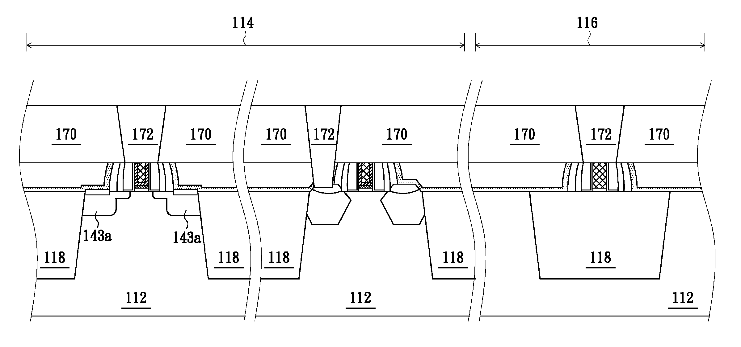
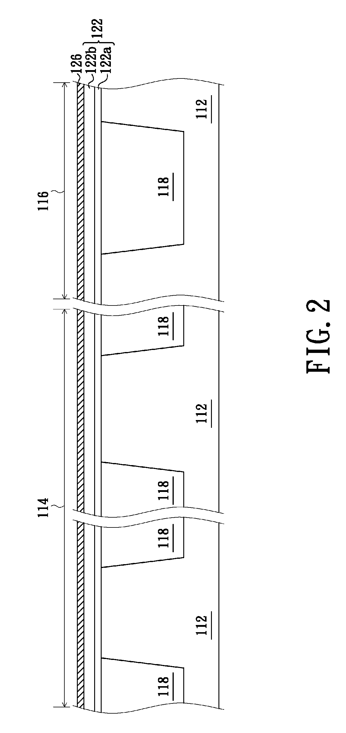
[0017]Referring to FIG. 2 through FIG. 9, FIGS. 2-9 illustrate a method of forming an electrical fuse and a metal gate transistor according to an embodiment of the present invention. The like numbered numerals designate similar or the same parts, regions or elements. It is to be understood that the drawings are not drawn to scale and are served only for illustration purposes. As shown in FIG. 2, a substrate 112, such as a silicon substrate, a silicon-containing substrate, or a silicon-on-insulator (SOI) substrate, is provid...


PUM


Abstract

The present invention provides a method of integrating an electrical fuse process into a high-k / metal gate process. The method simultaneously forms a dummy gate stack of a transistor and a dummy gate stack of an e-fuse; and simultaneously removes the polysilicon of the dummy gate stack in the transistor region and the polysilicon of the dummy gate stack in the e-fuse region. Thereafter, the work function metal layer disposed in the opening of the e-fuse region is removed; and the opening in the transistor region and the opening in the e-fuse region with metal conductive structures are filled to form an e-fuse and a metal gate of a transistor.

Description

BACKGROUND[0001]1. Field of the Invention[0002]The present invention relates to a method of forming an electrical fuse (e-fuse) and a metal gate transistor, and more particularly to a method of integrating an e-fuse process into a high dielectric constant (high-k) material and metal gate (HK / MG) process.[0003]2. Description of Related Art[0004]Electrical fuses (e-fuses) are generally applied to redundancy circuits in the integrated circuits. Once a defect is detected in the circuit, these e-fuses are used to trim or replace the defective part(s) of the circuit. In a conventional memory structure, some fuses are fabricated in the top metal layer. If some memory cells, word lines or lead wires fail, the fuses may be used to disconnect the failed parts, and some redundant memory cells, redundant word lines or redundant lead wires may replace the failed parts.[0005]In addition, some fuse designs can even provide the programming function. For example, each transistor of a memory array ma...

Claims


Application Information

Patent Timeline
Patent Type & Authority Patents(United States)
IPC IPC(8): H01L29/00
CPCH01L21/823807H01L21/823814H01L23/5256H01L27/0629H01L27/112H01L27/11206H01L29/7843H01L29/7848H01L2924/0002H01L2924/00H10B20/20H10B20/00
Inventor LIN, YUNG-CHANGWU, KUEI-SHENGWONG, CHANG-CHIEN
Owner UNITED MICROELECTRONICS CORP
Why Eureka
Try Eureka