Integrated structure of IGBT and diode and method of forming the same

a technology which is applied in the field of integrated structure of igbt and diodes and the same, can solve the problems of high production cost, complicated packaging, and large size, and achieve the effects of low cost, high withstand voltage, and high component density

Inactive Publication Date: 2010-12-02
ANPEC ELECTRONICS CORPORATION
View PDF12 Cites 9 Cited by
  • Summary
  • Abstract
  • Description
  • Claims
  • Application Information

AI Technical Summary

Benefits of technology

[0008]The present invention provides an integrated structure of an IGBT and a diode and a method of forming the same to satisfy device demands for lower cost, higher component density, higher withstand voltage, higher reliability, and higher yield.

Problems solved by technology

However, the structure, which includes IGBT connected to an external diode, has higher production cost, more complicated packaging, and is large in size, so it does not conform to a trend of high degree of integration for electronic components.
Therefore, integration of an IGBT and a diode in the same circuit structure has been developed in the industry, but it still faces several problems with existing integration methods and structures.
However, the thinner the thickness of the wafer is, the more difficult a delivery process in the apparatus for manufacturing doped regions is because the wafer tends to break.
Therefore, the current integration method suffers from low product yield, and the broken wafers may causes severe contaminations to the apparatus.
As a result, how to provide an integrated structure of an IGBT and a diode, for lower cost, higher component density, higher withstand voltage, higher reliability, and higher yield, is still a major issue.

Method used


Image

  • Integrated structure of IGBT and diode and method of forming the same
  • Integrated structure of IGBT and diode and method of forming the same
  • Integrated structure of IGBT and diode and method of forming the same

Examples


Embodiment Construction

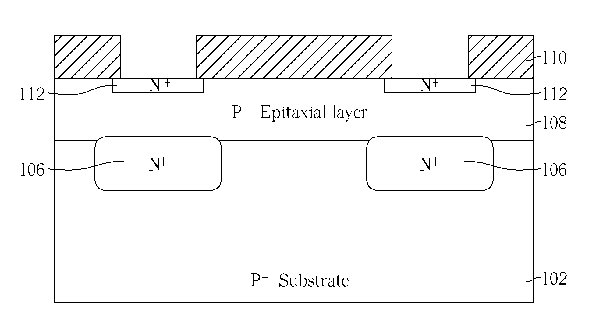
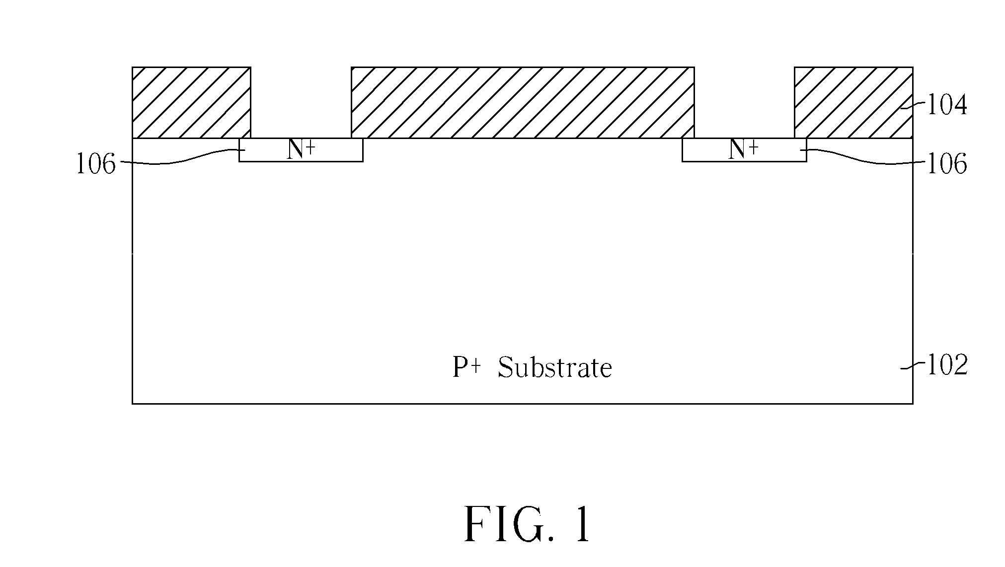
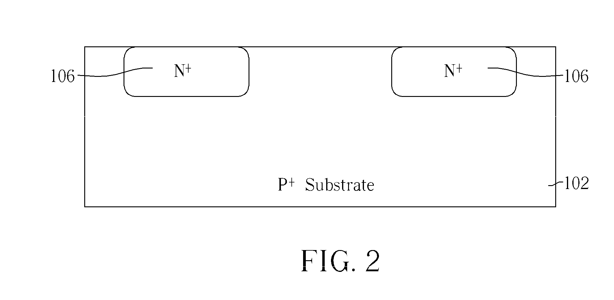
[0037]The present invention provides an integrated structure of an IGBT and a diode and a method of forming the same. The integrated structure has a plurality of doped regions which are overlapping with each other and serve as cathodes of diodes. The integrated structure can be utilized in the devices with high power or high frequency, but it is not limited herein. Please refer to FIGS. 1-9. FIGS. 1-9 are schematic diagrams illustrating a method of forming an integrated structure of an IGBT and a diode according to a first preferred embodiment of the present invention, wherein the same component or the same region is indicated as the same symbol. The first preferred embodiment is explained with an integrated structure of a trench punch-through IGBT and a diode, but the invention is not limited herein. It should be noted that the diagrams are for explanations and are not drawn as original sizes or to scale.

[0038]As shown in FIG. 1, a silicon substrate 102 is provided firstly, and a p...


PUM


Abstract

An integrated structure of an IGBT and a diode includes a plurality of doped cathode regions, and a method of forming the same is provided. The doped cathode regions are stacked in a semiconductor substrate, overlapping and contacting with each other. As compared with other doped cathode regions, the higher a doped cathode region is disposed, the larger implantation area the doped cathode region has. The doped cathode regions and the semiconductor substrate have different conductive types, and are applied as a cathode of the diode and a collector of the IGBT. The stacked doped cathode regions can increase the thinness of the cathode, and prevent the wafer from being overly thinned and broken.

Description

BACKGROUND OF THE INVENTION[0001]1. Field of the Invention[0002]This present invention is related to an integrated structure of an insulated gate bipolar transistor (IGBT) and a diode and a method of forming the same, and more particularly, to an integrated structure of an IGBT and a rectifier diode and a method of forming the same.[0003]2. Description of the Prior Art[0004]An IGBT is regarded as a composite structure combining a metal-oxide-semiconductor field effect transistor (MOSFET) and a bipolar junction transistor (BJT). By combining the MOSFET's characteristic of easy control with a gate electrode and the BJT's characteristic of low turn-on voltage drop, the IGBT is widely applied in a high voltage and high power application.[0005]Conventionally, the IGBT is formed on a substrate by semiconductor manufacturing technology. Then the IGBT is electrically connected to an external diode for providing a rectifier function, so that the circuit component of IGBT and the diode compon...

Claims


Application Information

Patent Timeline
Patent Type & Authority Applications(United States)
IPC IPC(8): H01L27/06H01L21/77
CPCH01L29/0834H01L29/7395H01L29/66333
Inventor LIN, WEI-CHIEHCHEN, HO-TAIYEH, JEN-HAOLIN, LI-CHENGHUNG, SHIH-CHIEH
Owner ANPEC ELECTRONICS CORPORATION
Why Eureka
Try Eureka