Method of forming low dielectric constant interlayer dielectric film

A technology of low dielectric constant layer and dielectric thin film, which is applied in coatings, circuits, electrical components, etc., can solve problems including the combination of thin films, mechanical and electrical properties, and achieve the effects of safe handling, easy acquisition, and easy formation

Inactive Publication Date: 2005-07-27
VERSUM MATERIALS US LLC
View PDF14 Cites 14 Cited by
  • Summary
  • Abstract
  • Description
  • Claims
  • Application Information

AI Technical Summary

Problems solved by technology

One problem: it is difficult to include all the atoms or functionalities needed in the film in the same precursor molecule and have them present in the desired proportions to produce Si a o b C c h d or Si a o b C c h d f e Thin film, wherein the total atomic % of a+b+c+d+e=100%, and a=10-35%, b=1-66%, c=1-35%, d=0-60%, e = 0-25%
[0029] Despite the above developments, there are still no examples in the prior art of successfully combining the desired mechanical and electrical properties that are most important for incorporating low-k dielectric materials into integrated circuits

Method used


Image

  • Method of forming low dielectric constant interlayer dielectric film
  • Method of forming low dielectric constant interlayer dielectric film
  • Method of forming low dielectric constant interlayer dielectric film

Examples


Embodiment

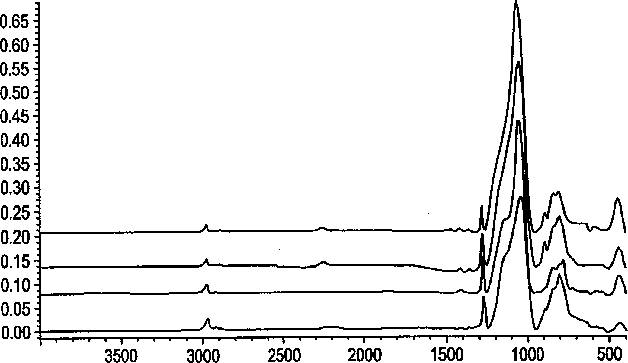
[0098] All experiments were performed in a 200 mm DxZ chamber equipped with an Advance Energy 2000rf generator on an Applied Materials Precision-5000 system using a dopant-free TEOS process kit. The experimental method included the following basic steps: initial setting and stabilization of the gas flow, supply of RF energy to generate the plasma and induce deposition, and purge / evacuate the chamber before removing the wafer. Subsequently, after each deposition with in-place C 2 f 6 +O 2 The cleaning of the chamber is followed by a step of drying the chamber.

[0099] The dielectric constants of low resistivity p-type wafers (<0.02 ohm-cm) were determined using the Hg probe technique. Transmission infrared spectroscopy was performed on high resistivity wafers and all data were normalized based on film thickness. Thickness and refractive index were measured by reflectometer with 5 point average. Adhesion was measured with a tape pull test. Mechanical properties (such as Y...

Embodiment 7

[0122] A contemplated embodiment of the invention based on the use of dimethoxymethylsilane (DMOMS) as the organosilane precursor for a 200 mm silicon wafer substrate is shown in Table 8 below.

[0123] Room pressure (Torr)

[0124] It is expected that the k value will be in the range of 2.7-3.0, the Young's modulus is about 15 GPa, and the nanoindentation hardness is about 2 GPa.

[0125] A contemplated embodiment of the invention based on the use of phenoxydimethylsilane (PODMS) as the organosilane precursor for a 200 mm silicon wafer substrate is shown in Table 9 below.

[0126] Room pressure (Torr)

[0127] It is expected that the k value will be in the range of 2.7-3.0, the Young's modulus is about 15 GPa, and the nanoindentation hardness is about 2 GPa.

[0128] A contemplated embodiment of the invention based on the use of di-tert-butoxymethylsilane (DTBMS) as the organosilane precursor for a 200 mm silicon wafer substrate is shown in Table 10 below....


PUM

PropertyMeasurementUnit
hardnessaaaaaaaaaa
hardnessaaaaaaaaaa
hardnessaaaaaaaaaa

Abstract

The present invention relates to a method of forming a low dielectric constant interlayer dielectric film, the method comprising, under chemical vapor deposition conditions sufficient to deposit the film on a substrate, an organosilicon precursor comprising one or more organosilicon compounds, Optionally react with one or more other reactive substances to form an interlayer dielectric film with a dielectric constant of 3.5 or lower, the organosilicon compound containing one or more selected from C2-C10 epoxy, C2-C8 carboxylates, C2-C8 alkynes, C4-C8 dienes, C3-C5 strained ring groups, and reactive side groups of C4-C10 groups that can sterically hinder or strain silicone precursor. The invention also relates to films formed by the above methods.

Description

[0001] This application is a divisional application of the parent case whose application number is CN02102345.X. The filing date of the parent application is January 17, 2002; the title of the invention is "organic silicon precursor for low dielectric constant interlayer dielectric film". technical field [0002] The invention relates to a method for forming a low dielectric constant interlayer dielectric thin film on a substrate by chemical vapor deposition (CVD) using a specific organosilicon precursor. Background technique [0003] The electronics industry utilizes dielectric materials as insulating layers between circuits and components of integrated circuits (ICs) and associated electronic devices. To increase the speed and memory capacity of microelectronic devices such as computer chips, the size of the circuits is decreasing. The size of microchips has been greatly reduced in the past decade, and the line width of about ...

Claims


Application Information

Patent Timeline
Patent Type & Authority Applications(China)
IPC IPC(8): B05D7/24C23C16/40H01L21/312H01L21/316H01L21/768H01L23/522
CPCH01L21/31633C09D183/06H01L21/02274H01L21/3121H01L21/31629H01L21/02216H01L21/02126H01L21/02131B05D1/60C23C16/401H01L21/02211
Inventor J·L·文森特M·L·奥内尔小H·P·威瑟斯S·E·贝克R·N·弗蒂斯
Owner VERSUM MATERIALS US LLC
Why Eureka
Try Eureka