Plasma display panel

一种显示面板、等离子体的技术,应用在交流电等离子显示板、气体放电电极、固体阴极零部件等方向,能够解决电极电压降驱动速度和响应时间衰减、图像残留、发光效率降低等问题

Inactive Publication Date: 2005-11-02
SAMSUNG SDI CO LTD
View PDF2 Cites 1 Cited by
  • Summary
  • Abstract
  • Description
  • Claims
  • Application Information

AI Technical Summary

Problems solved by technology

As a result, a lot of visible light cannot reach the outside of the display, so the luminous efficiency is reduced
[0009] With electrodes on the front panel, the plasma must start near the front panel side of the discharge cell, which creates a difficult-to-use and inefficient discharge
Also, this arrangement of electrodes and phosphor layer also results in sputtering of ions from the plasma onto the phosphor layer, especially when the same image is observed for a long time, resulting in permanent image retention
[0010] When electrodes are placed on the front substrate, transparent but highly resistive materials are also used for the electrodes, thus causing a voltage drop along the electrodes and degradation of drive speed and response time

Method used


Image

  • Plasma display panel
  • Plasma display panel
  • Plasma display panel

Examples


Embodiment Construction

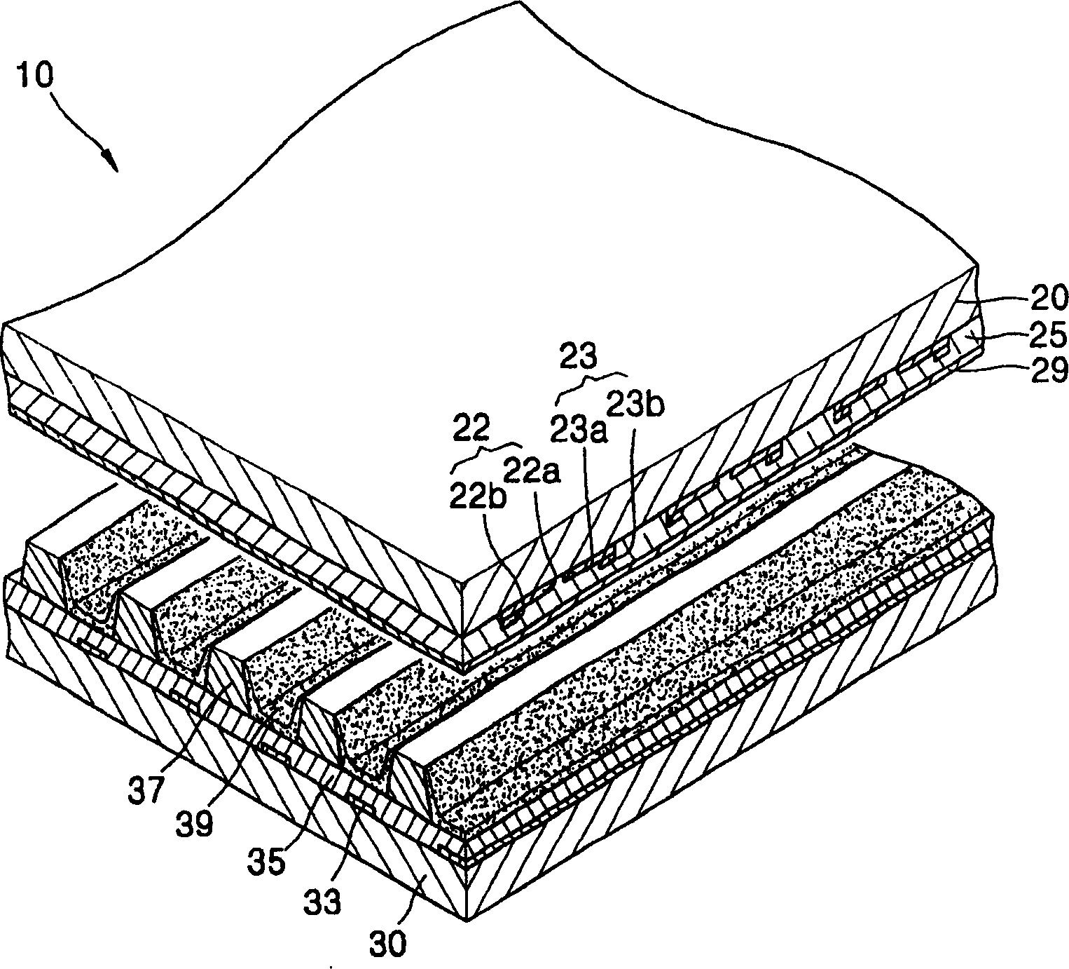
[0030] Referring now to the drawings, FIG. 1 depicts a three-electrode surface discharge AC PDP 10 similar to that disclosed in, for example, US Patent No. 6,753,645 to Haruki et al. Referring to FIG. 1 , a three-electrode surface discharge AC-PDP 10 includes a front panel 20 and a rear panel 30 .

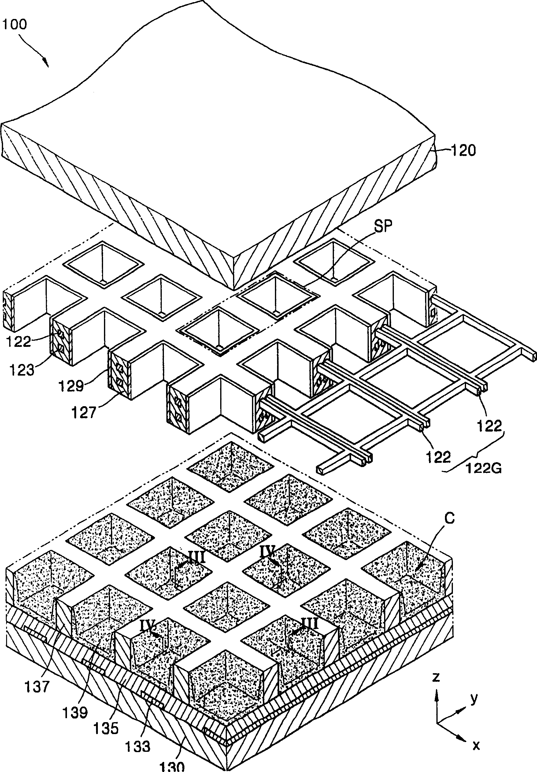
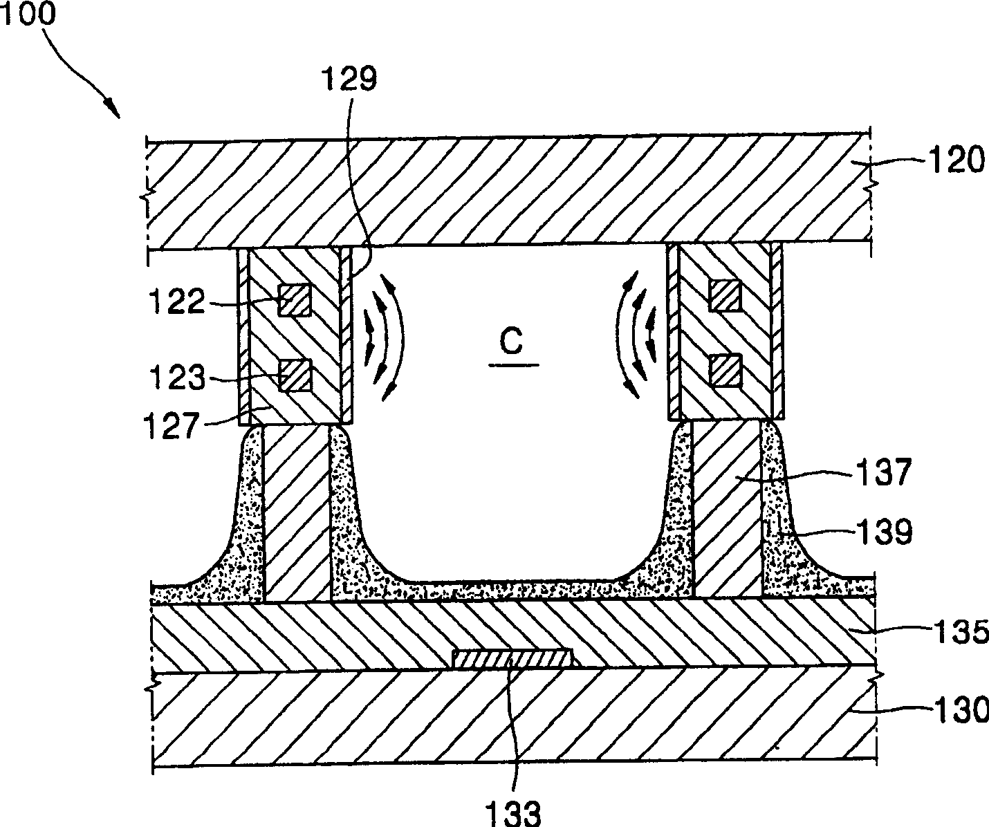
[0031] On the rear plate 30, the address electrodes 33 that generate the address discharge, the rear dielectric layer 35 that covers the address electrodes 33, the partition walls 37 that define the discharge cells, and the side walls that are arranged on the partition walls 37 and the absence of the rear plate 30 are arranged. The phosphor layer 39 on the portion covered by the partition wall 37 .

[0032] On the front plate 20 facing and separated from the rear plate 30, X-electrodes 22 and Y-electrodes 23 generating sustain discharges, a front dielectric layer 25 covering the X-electrodes 22 and Y-electrodes 23, and protective layer29. Here, the X-electrode 22 may include a tr...


PUM


Abstract

A plasma display panel having a plurality of pixels, each pixel having at least three sub-pixels, each sub-pixel containing at least two discharge cells. The plasma display panel includes a transparent front panel, a back panel positioned to be separate from and parallel to the front panel, first barrier ribs located between the front panel and the back panel and defining discharge cells together with the front panel and the back panel, the first barrier ribs being made out of a dielectric material, front discharge electrodes located within the first barrier ribs and surrounding the discharge cells, back discharge electrodes also located within the first barrier ribs and also surrounding the discharge cells and being separated from the front discharge electrodes, phosphor layers located within the discharge cells, respectively, and a discharge gas present within the discharge cells.

Description

[0001] priority claim [0002] This application is hereby incorporated by reference under 35 U.S.C §119 and is claimed to have been filed in the Korean Patent Office on April 28, 2004, entitled "PLASMA DISPLAY PANEL" (Plasma Display Panel), Serial No. 10 - All rights to the application of 2004-0029649. technical field [0003] The present invention relates to a plasma display panel (PDP), and more particularly, to a PDP capable of improving luminous efficiency and efficiently operating with a low driving voltage. Background technique [0004] The PDP flat panel display is thin, light in weight, has a large screen, has good display quality, and has a wide viewing angle. In addition, PIDPs are simple to manufacture and can be made into large sizes compared to other flat panel display devices. Therefore, the PDP is considered to be a next-generation large-size flat panel display device. [0005] According to an applied discharge voltage, the PDP is classified into a direct c...

Claims


Application Information

Patent Timeline
Patent Type & Authority Applications(China)
IPC IPC(8): H01J11/16H01J11/22H01J11/24H01J11/32H01J11/34H01J11/36
CPCH01J11/24H01J2211/361H01J11/16H01J2211/245H01J11/36A63C19/04A63C19/10
Inventor 金禹泰姜景斗金世宗
Owner SAMSUNG SDI CO LTD
Why Eureka
Try Eureka