Active matrix electroluminescent display devices

An electroluminescent display, active matrix technology, applied in static indicators, instruments, etc., can solve problems such as difficulties

Inactive Publication Date: 2006-03-01
KONINKLIJKE PHILIPS ELECTRONICS NV
View PDF1 Cites 31 Cited by
  • Summary
  • Abstract
  • Description
  • Claims
  • Application Information

AI Technical Summary

Problems solved by technology

[0012] Thus, there are difficulties in implementing addressing schemes suitable for pixels with amorphous silicon TFTs, and even fluorescent LED displays

Method used


Image

  • Active matrix electroluminescent display devices
  • Active matrix electroluminescent display devices
  • Active matrix electroluminescent display devices

Examples


Embodiment Construction

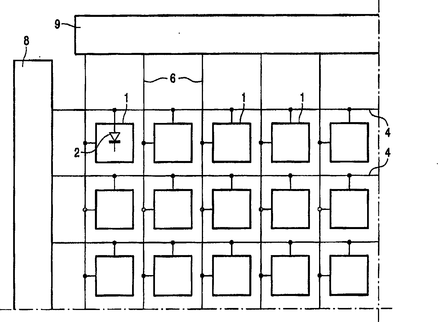
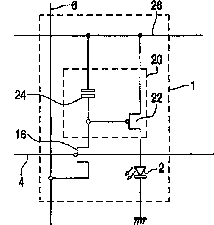
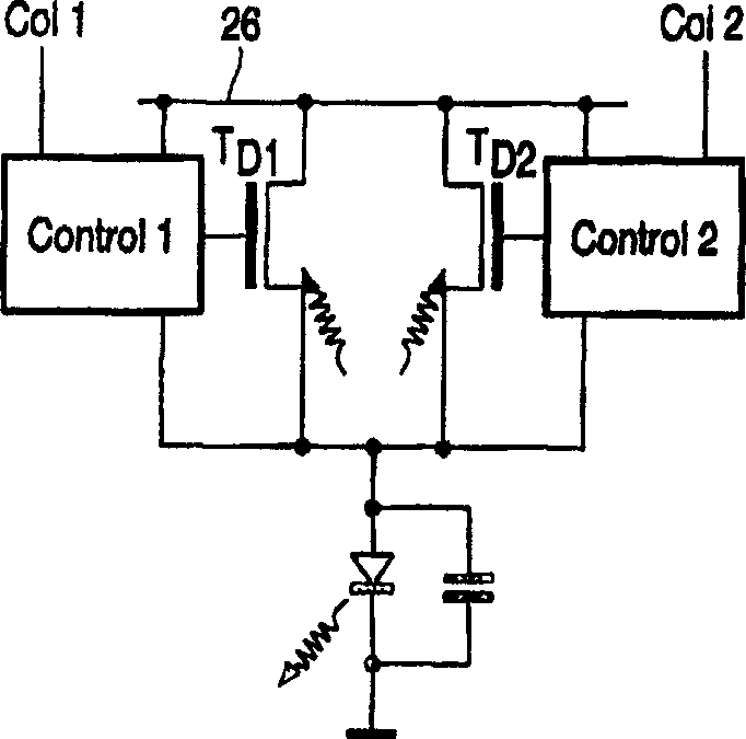
[0065] The present invention restores the characteristics of the amorphous silicon TFT by providing more than one current supply TFT for each pixel, so that one TFT supplies current to the LED, and the other driving TFTs are in a cut-off state. These TFTs were also irradiated to enhance the recovery process.

[0066] image 3 and 4 The basic principle on which the invention is based is schematically illustrated.

[0067] image 3 Indicates two drive TFTs used to drive the anode of the LED display element T D1 and T D2 . Each drive transistor is controlled by a corresponding control circuit "Control 1" and "Control 2" which receives data input along a corresponding column line "Col1" and "Col2". Figure 4 Indicates two drive TFTs used to drive the cathode of the LED display element T D1 and T D2 . This is more difficult to achieve, but is more suitable for N-type circuits. image 3 and 4 A circuit with two drive transistors is shown schematically, although more than two...


PUM


Abstract

Each pixel of an active matrix electroluminescent display device has a first amorphous silicon drive transistor for intermittently driving a current through the display element and a second amorphous silicon drive transistor for intermittently driving a current through the display element. The aging effect of amorphous silicon TFTs can be reduced by sharing the driving of the display element between two drive transistors. Providing a duty cycle reduces the on-time for each drive transistor, but also provides a period during which there can be some recovery of the TFT characteristics.

Description

technical field [0001] The present invention relates to electroluminescent display devices, in particular active matrix display devices having a thin film switching transistor associated with each pixel. Background technique [0002] Matrix display devices employing electroluminescent light-emitting display elements are well known. The display elements may include, for example, organic thin film electroluminescent elements using polymer materials, or light emitting diodes (LEDs) using conventional III-V semiconductor compounds. Recent research on organic electroluminescent materials, especially polymer materials, has shown that they can be practically used in video display devices. These materials typically include one or more layers of semiconducting conjugated polymers sandwiched between a pair of electrodes, one of which is transparent and the other has a material suitable for injecting holes or electrons into the polymer layer. Organic electroluminescent materials exhi...

Claims


Application Information

Patent Timeline
Patent Type & Authority Applications(China)
IPC IPC(8): G09G3/32
CPCG09G2300/0852G09G2300/0861G09G2320/043G09G2300/0809G09G2310/0251G09G2300/0866G09G3/3233G09G2300/0417G09G2300/0819G09G2310/063G09G2310/0254G09G2310/0256G09G3/30G09G3/32G09G3/20
Inventor S·C·迪恩D·A·费什A·G·克纳普
Owner KONINKLIJKE PHILIPS ELECTRONICS NV
Why Eureka
Try Eureka