

Solid immersion lens and microscope
An immersion lens and microscope technology, applied in microscopes, lenses, instruments, etc., can solve the problem of electronic device inspection requiring a lot of labor and time.
- Summary
- Abstract
- Description
- Claims
- Application Information
AI Technical Summary
Problems solved by technology
Method used
Image

Examples
Embodiment Construction
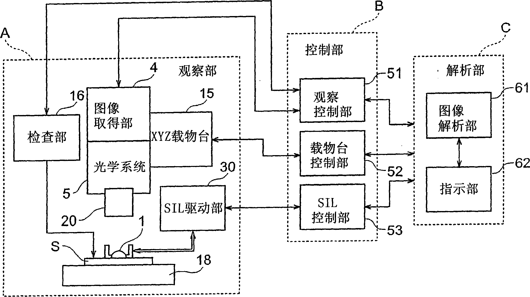
[0042] Preferred embodiments of the present invention will be described below with reference to the drawings. In addition, in each embodiment, the same code|symbol is attached|subjected to the part which has the same function, and overlapping description is abbreviate|omitted. In addition, the dimensional ratios of the drawings do not necessarily match those described.
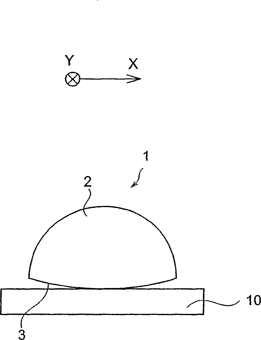
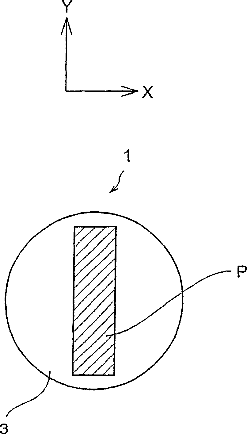
[0043] Figure 1A and Figure 1B It shows the state after mounting the immersion lens of this embodiment on a semiconductor substrate, Figure 1A is a side view, Figure 1B It is a rear view.
[0044] The immersion lens 1 of this embodiment is mounted on a substrate of a semiconductor device to be observed (inspected) during use. When analyzing the back surface of a semiconductor device using an immersion lens, the semiconductor substrate itself is utilized as a part of the immersion lens by optically coupling the immersion lens to the semiconductor substrate. In this way, when the focus of the objective...
PUM
 Abstract
Description
Claims
Application Information