
Voltage level converter

A voltage level, voltage source technology, applied in the direction of logic circuit connection/interface layout, logic circuit coupling/interface using field effect transistors, etc., can solve the problems of slow switching speed, thick gate, high threshold voltage, etc. and jitter reduction effect

Active Publication Date: 2006-04-26
VIA TECH INC
View PDF0 Cites 13 Cited by
  • Summary
  • Abstract
  • Description
  • Claims
  • Application Information

AI Technical Summary

Problems solved by technology

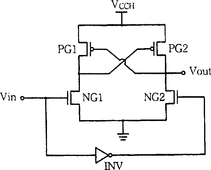
[0005] In addition, since the highest voltage that the NMOS transistors NG1 and NG2 can withstand is about 2.5 volts, the gate must be made thicker, so the threshold voltage is also higher
At this time, the lower input voltage Vin cannot turn on the NMOS transistors NG1 and NG2, so the switching speed of the NMOS transistors NG1 and NG2 is slow

Method used


Image

  • Voltage level converter
  • Voltage level converter
  • Voltage level converter

Examples


Embodiment Construction

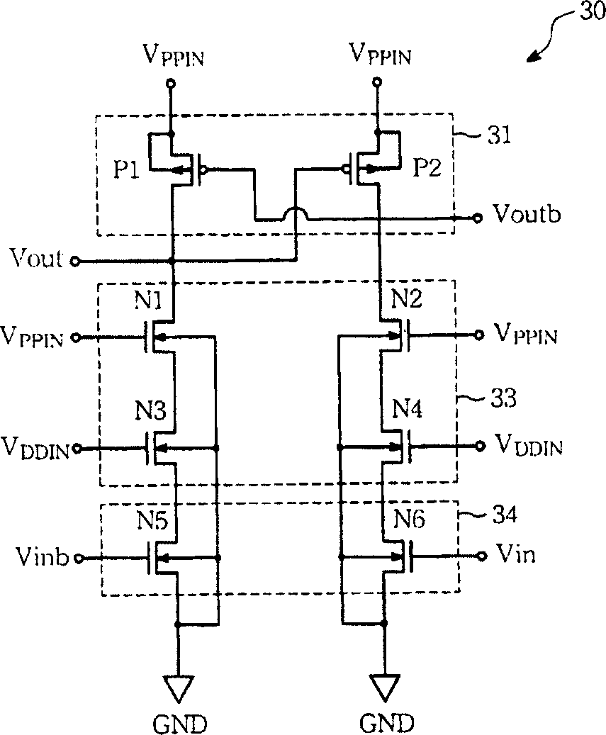
[0033] see image 3 , shows an embodiment of the voltage level shifter of the present invention. As shown in the figure, the voltage level shifter 30 has a pull-up circuit 31, a voltage drop circuit 33, and a pull-down circuit 34, the pull-up circuit 31 has two PMOS transistors P1 and P2, and the voltage drop circuit 33 has There are four NMOS transistors N1, N2, N3 and N4, and the pull-down circuit 34 has two NMOS transistors N5 and N6. In this embodiment, a DC voltage VPPIN and a DC voltage source VDDIN are provided as the operating voltage of the voltage level shifter 30, and the NMOS transistors N5 and N6 are connected to the ground GND for driving the voltage level shifter 30 to An input voltage Vin is converted into an output voltage Vout, wherein the DC voltage VPPIN is 3.3 volts, the DC voltage VDDIN is 1.2 volts, the input voltage Vin is a rectangular wave between 0 volts and 1.2 volts, and the output voltage Vout is between 0 volts and the corresponding wave betwee...


PUM


Abstract

The disclosed voltage-level translator, which comprises a draw-up circuit, a path cutting circuit to separate the draw-up / down circuits when translating, a voltage drop circuit, and a draw-down circuit constructed by thin-grid transistor for the low received voltage to improve switch speed. This invention avoids the competition between draw-up and down circuits, and reduces output voltage noise and jitter.

Description

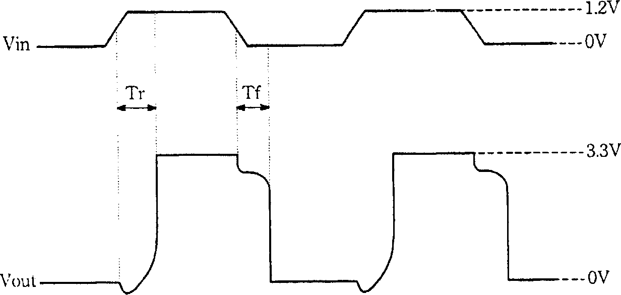
technical field [0001] The invention relates to a voltage level shifter, in particular to a voltage level shifter capable of reducing noise and jitter phenomena at an output end. Background technique [0002] As far as modern integrated circuit systems are concerned, their core logic units and I / O units usually use two different supply voltages. Taking the 0.13 μm process as an example, the core logic unit is usually supplied with a voltage of 1.2 volts, while the I / O unit is usually supplied with a voltage of 3.3 volts. Due to the different operating voltages, a conversion circuit is required between the core logic unit and the I / O unit to convert the 1.2 volts to 3.3 volts. This conversion circuit is generally called a "voltage level converter". [0003] figure 1 Shown is a conventional voltage level shifter 10, which includes PMOS transistors PG1 and PG2, NMOS transistors NG1 and NG2, and an inverter INV, wherein the PMOS transistors PG1 and PG2 are called pull-up trans...

Claims


Application Information

Patent Timeline
IPC IPC(8): H03K19/0175H03K19/0185
Inventor 黄超圣
Owner VIA TECH INC
Learn More