Method and apparatus for testing integrated circuits

A test module and test system technology, applied in the direction of digital circuit test, electronic circuit test, etc., can solve problems such as impossibility of plug and play, and achieve the effects of reduced test cost, reduced work intensity, and faster turnaround time

Inactive Publication Date: 2006-05-17
ADVANTEST CORP
View PDF0 Cites 11 Cited by
  • Summary
  • Abstract
  • Description
  • Claims
  • Application Information

AI Technical Summary

Problems solved by technology

However, due to the proprietary nature of conventional test systems and the proprietary nature of the

Method used


Image

  • Method and apparatus for testing integrated circuits
  • Method and apparatus for testing integrated circuits
  • Method and apparatus for testing integrated circuits

Examples


Embodiment Construction

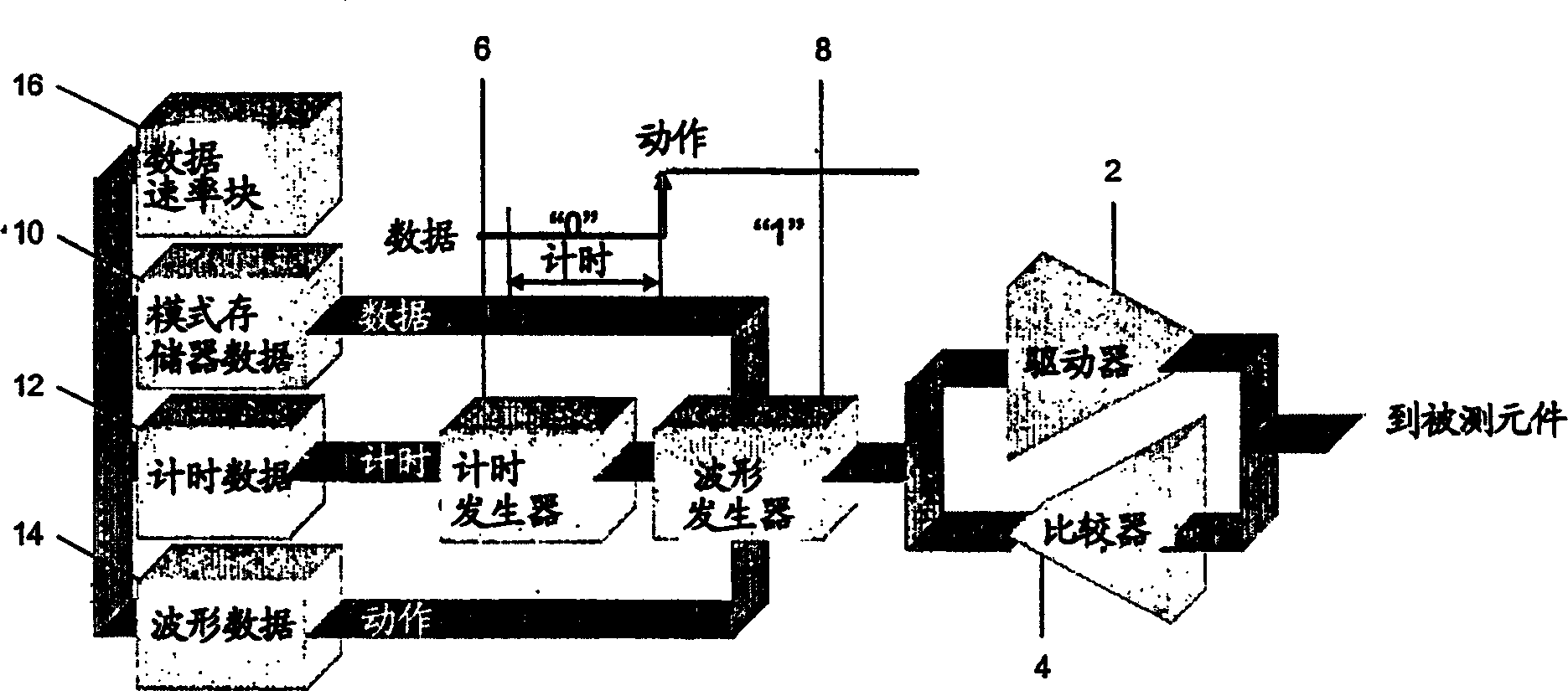
[0034] Figure 1 shows the general architecture of a conventional tester, showing how signals are generated and applied to the device under test (DUT). Each DUT input pin is connected to a driver 2 that applies test data, while each DUT output pin is connected to a comparator 4 (comparator). In most cases, use tri-state driver-comparators (tri-state driver-comparators), so that each test pin (channel) can be used as both an input pin and an output pin. A collection of test pins for a single DUT forms a test site, which is associated with an associated timing generator 6 (timing generator), waveform generator 8 (waveform generator), and pattern memory 10 (pattern memory) , timing data memory 12 (timing data memory), waveform storage data 14 (waveform memory data) and block 16 (block) defining the data rate (data rate) work together.

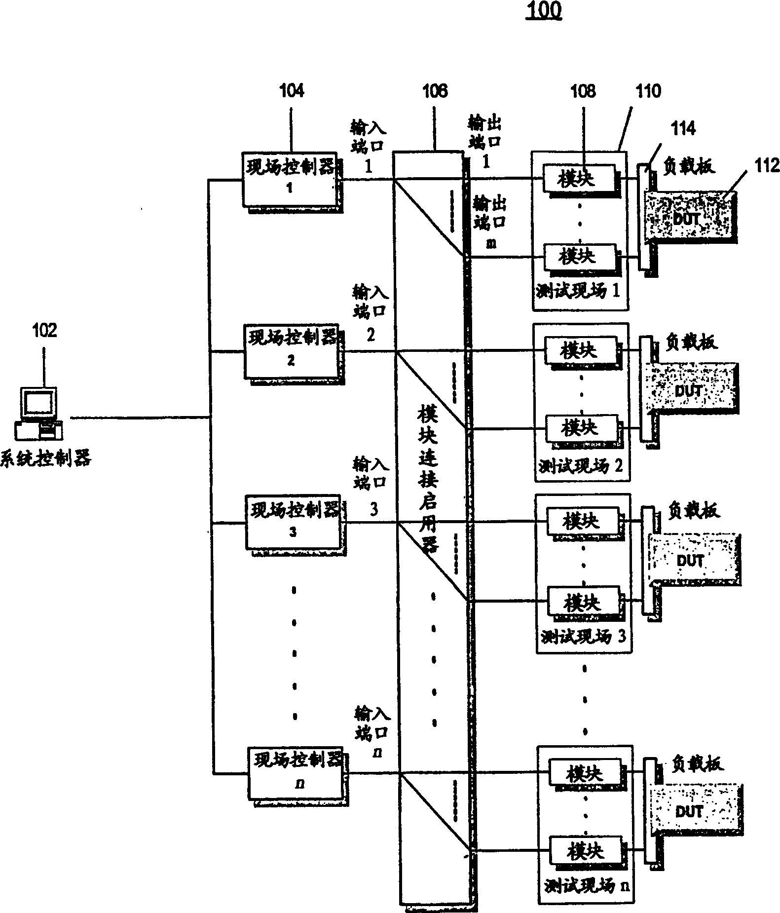
[0035] figure 2 Shown is a system architecture 100 according to an embodiment of the invention. A system controller (SysC) 102 is coupled to a ...


PUM


Abstract

The present invention describes a distributed operating system for semiconductor test systems, such as automated test equipment (ATE). The operating system includes a main operating system for controlling one or more field controllers through a system controller. One or more local operating systems, each associated with an on-site controller, control the one or more test modules through an associated on-site controller. Each test module performs a test on a corresponding DUT at a test site.

Description

technical field [0001] The present invention relates to the testing of integrated circuits (ICs), and more particularly to automated test equipment (ATE) for testing one or more ICs. Background technique [0002] This application claims priority to the following applications: Application Serial No. 60 / 449,622, filed February 24, 2003, entitled "Method and Apparatus for Testing Integrated Circuits"; 60 / 447,839, entitled "Methods and Structures for Developing Test Programs for Semiconductor Integrated Circuits"; U.S. Application Serial No. 10 / 404,002, filed March 31, 2003, entitled "Test Simulators, Test Module Simulators, and Recording Media Storage Programs Therein"; US Application Serial No. 10 / 403,817, filed March 31, 2003, entitled "Test Apparatus and Test Method," all of which are hereby incorporated by reference in their entirety. This application also makes reference in its entirety to concurrently filed U.S. Application No. _________, entitled "Method and Structure f...

Claims


Application Information

Patent Timeline
IPC IPC(8): G01R31/319
Inventor 安肯·拉马尼克马克·艾尔斯顿陈良力罗伯·萨乌尔
Owner ADVANTEST CORP
Why Eureka
Try Eureka