Semiconductor device and fabrication method thereof

A semiconductor and device technology, applied in the field of semiconductor devices and their manufacturing process, can solve the problem of increased hole mobility

Active Publication Date: 2006-07-05
SOCIONEXT INC
View PDF2 Cites 39 Cited by
  • Summary
  • Abstract
  • Description
  • Claims
  • Application Information

AI Technical Summary

Problems solved by technology

Therefore, this increases the mobility of holes in the channel regi

Method used


Image

  • Semiconductor device and fabrication method thereof
  • Semiconductor device and fabrication method thereof
  • Semiconductor device and fabrication method thereof

Examples


no. 1 example

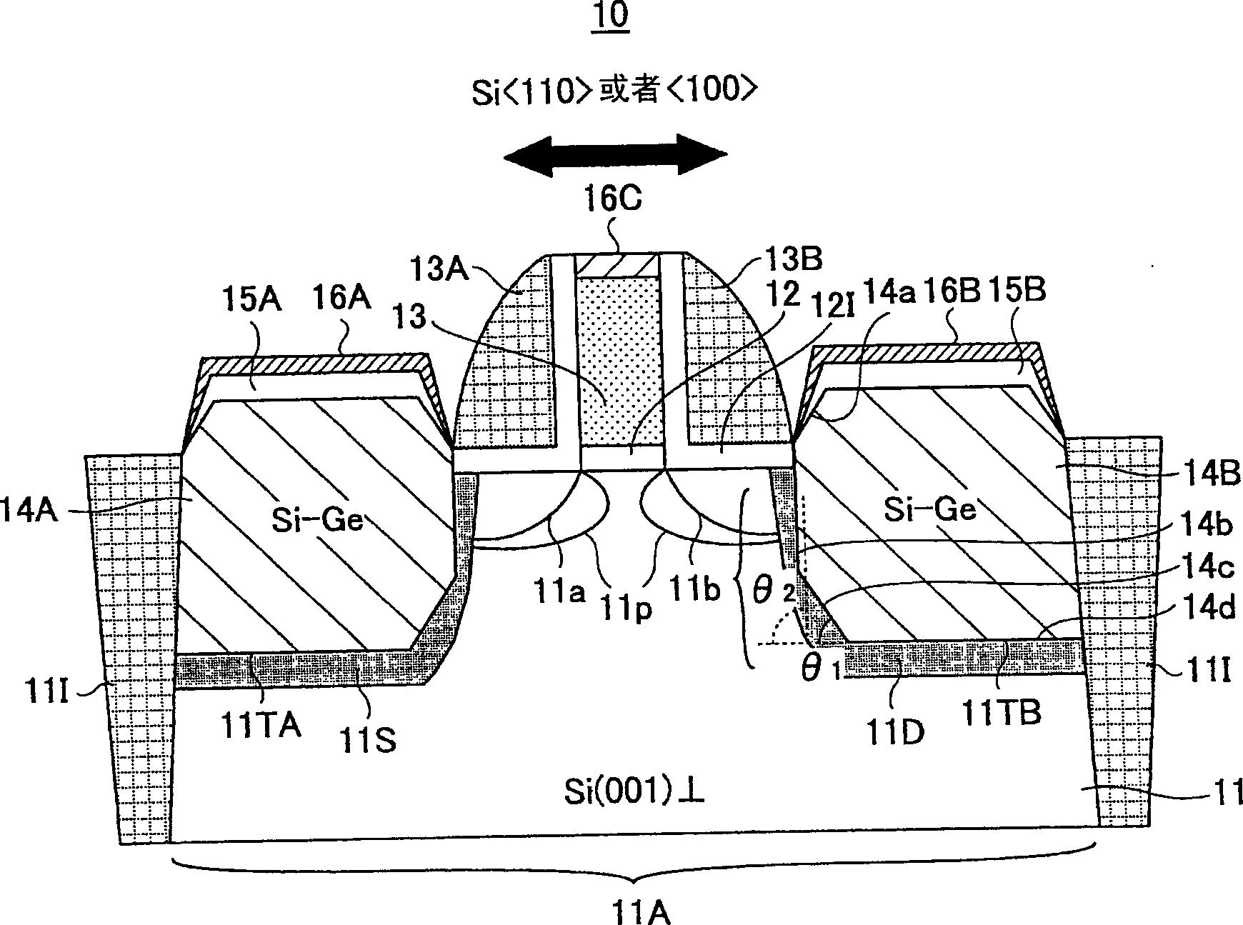
[0081] image 3 The structure of the P-channel MOS transistor 10 according to the first embodiment of the present invention is shown.

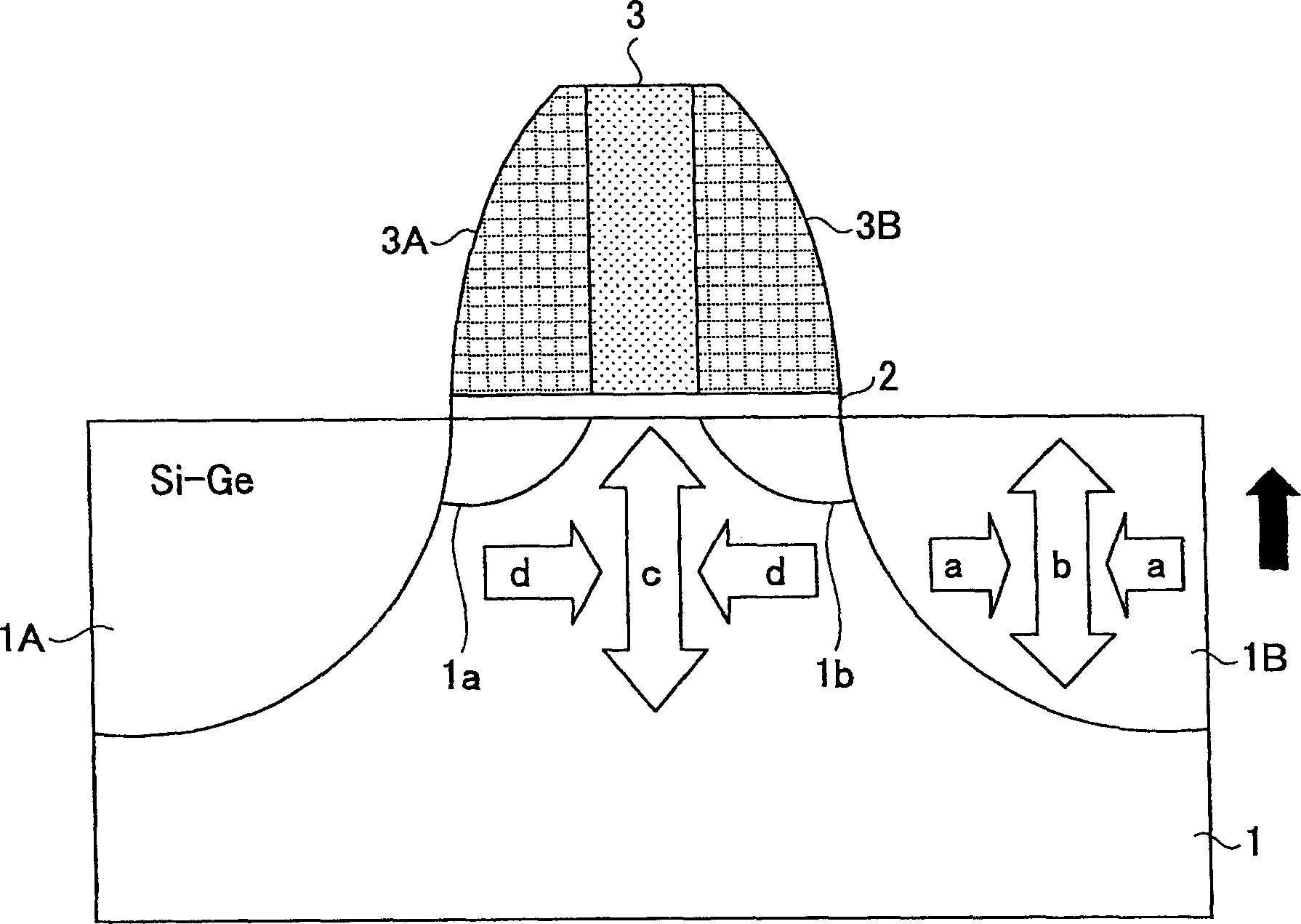
[0082] refer to image 3 , the P-channel MOS transistor 10 is formed on the n-type device region 11A defined by the STI device isolation region 11I on the silicon substrate in the (001) plane direction, wherein the high-quality gate insulating film of a thermal oxide film or a SiON film 12 is formed on the silicon substrate 11 corresponding to the channel region in the device region 11A, and has a thickness of about 1.2 nm.

[0083] In the above-mentioned device region 11A, a p-type doped polysilicon gate electrode 13 is formed on the gate insulating film 11 , wherein the silicon substrate surface exposed at lateral sides of the gate electrode 13 is covered by a CVD oxide film 12I. Therefore, it should be noted that each CVD oxide film 12I extends continuously, and covers the side wall surface of gate electrode 13 . Further, sidewall insula...

no. 2 example

[0118] will later refer to Figure 8A to Figure 8E explained Figure 4D The fabrication process of p-channel MOS transistors.

[0119] refer to Figure 8A , the device region 11A is defined on the surface of the p-type silicon substrate 11 by the STI-type device isolation structure 11I, and an n-type well is formed in the device region 11A by implanting n-type impurity elements into the device region 11A.

[0120] and, in Figure 8B In the step of , since the SiON film and polysilicon film patterned uniformly formed on the silicon substrate 11, a gate insulating film 12 and a polysilicon gate electrode 13 are formed on the silicon substrate 11 corresponding to the device region 11A, and by implanting p Type impurity elements such as B + , while using the polysilicon gate electrode 13 as a mask, a p-type source extension region 11a and a p-type drain extension region 11b are formed in the device region 11A.

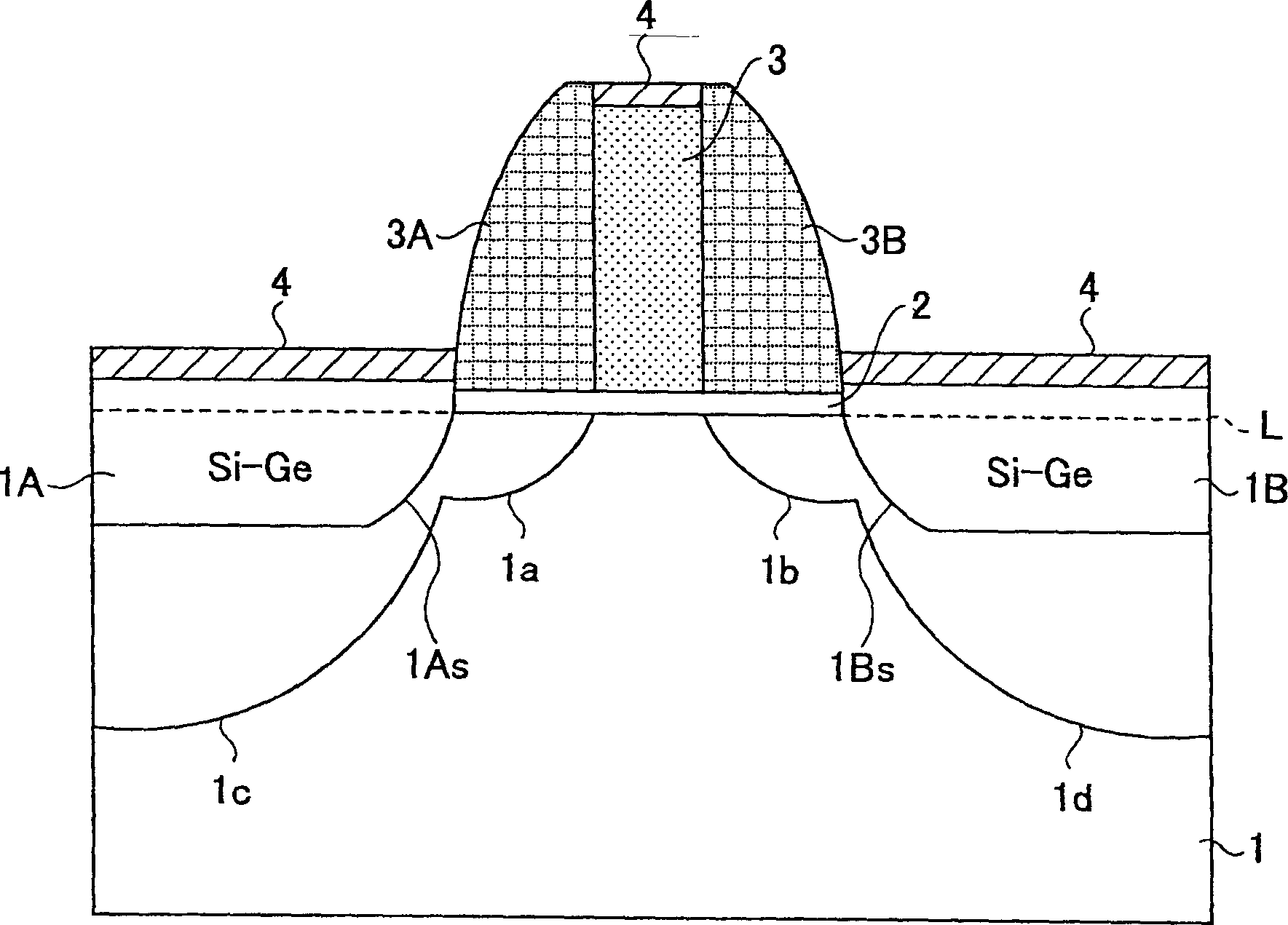
[0121] In addition, after the sidewall insulating films 13A and ...

no. 3 example

[0148] Figure 10A is an illustration of performing the process of FIG. 8D in a low-pressure CVD apparatus as a third embodiment of the present invention, summarizing the above-explained.

[0149] refer to Figure 10A , first, the substrate to be processed is introduced into a low-pressure CVD apparatus at a temperature of 400° C. or lower, and the temperature is raised to a predetermined processing temperature of 400-550° C. in a hydrogen atmosphere (heating).

[0150] Subsequently, in the same hydrogen atmosphere, at the same processing temperature, the substrate to be processed is kept for a maximum of 5 minutes, and a hydrogen heat treatment process (H 2 - baking).

[0151] Next, at the same process temperature, the process gas introduced into the low-pressure CVD apparatus was changed, and as described above, epitaxial growth (SiGe deposition) of p-type SiGe mixed crystal regions 14A and 14B was performed in trenches 11TA and 11TB .

[0152] and, in Figure 10A In th...


PUM

PropertyMeasurementUnit
Thicknessaaaaaaaaaa
Thicknessaaaaaaaaaa
Thicknessaaaaaaaaaa

Abstract

A semiconductor device includes a gate electrode formed on a silicon substrate via a gate insulation film in correspondence to a channel region, source and drain regions of a p-type diffusion region formed in the silicon substrate at respective outer sides of sidewall insulation films of the gate electrode, and a pair of SiGe mixed crystal regions formed in the silicon substrate at respective outer sides of the sidewall insulation films in epitaxial relationship to the silicon substrate, the SiGe mixed crystal regions being defined by respective sidewall surfaces facing with each other, wherein, in each of the SiGe mixed crystal regions, the sidewall surface is defined by a plurality of facets forming respective, mutually different angles with respect to a principal surface of the silicon substrate.

Description

[0001] related application [0002] This application is based on Japanese Priority Application No. 2004-380619 filed on December 28, 2004, the entire contents of which are incorporated herein by reference. technical field [0003] The present invention relates generally to semiconductor devices, and more particularly to a semiconductor device having increased operating speed due to pressure application and a process for manufacturing the same. Background technique [0004] With the development of device miniaturization technology, it is now possible to manufacture very small and ultra-high-speed semiconductor devices with a gate length of 100 nm or less. [0005] In this very small and ultra-high-speed transistor, the area of ​​the channel region directly below the gate is reduced compared to conventional semiconductor devices, and the mobility of electrons or holes passing through the channel region is limited by the force applied to this channel region. severe effects of ...

Claims


Application Information

Patent Timeline
IPC IPC(8): H01L29/78H01L21/336H01L21/205
CPCY10S257/90H01L29/66628H01L21/02639H01L29/7833H01L29/665H01L29/7848H01L21/30608H01L21/02381H01L29/78H01L29/66636H01L21/0262H01L29/165H01L29/045H01L29/0847H01L21/02532H01L21/02579H01L29/7842H01L21/28518H01L29/0653H01L29/45H01L29/4975H01L29/518
Inventor 岛宗洋介片上朗畑田明良岛昌司田村直义
Owner SOCIONEXT INC
Why Eureka
Try Eureka