Method and apparatus for implementing PCB design

A design drawing and design tool technology, applied in computing, special data processing applications, instruments, etc., can solve the problems of layout and wiring design plane renderings judgment error affecting the correctness of PCB design renderings, high error probability, and high PCB design cost

Inactive Publication Date: 2006-07-19
HUAWEI TECH CO LTD
View PDF0 Cites 6 Cited by
  • Summary
  • Abstract
  • Description
  • Claims
  • Application Information

AI Technical Summary

Problems solved by technology

[0012] In the above process of PCB design based on the structure diagram, whether the PCB designer's understanding of the structure diagram is correct, whether the PCB designer draws the outline drawing according to the structure diagram and the prohibited layout and wiring area are correct, whether the PCB layout and wiring design is correct, Judgment errors and human judgment errors brought about by plane renderings will affect the correctness of PCB design renderings
Once an error occurs in one of the steps, the process of drawing and judging the PCB design effect diagram will be repeated, resulting in a waste of PCB design time, thereby delaying the time to market of the product
[0013] To sum up, the existing method of PCB design based on the structural diagram, because too many human factors will increase the probability of errors in the entire PCB design process, resulting in low PCB design efficiency and high PCB design costs

Method used


Image

  • Method and apparatus for implementing PCB design
  • Method and apparatus for implementing PCB design
  • Method and apparatus for implementing PCB design

Examples


Embodiment Construction

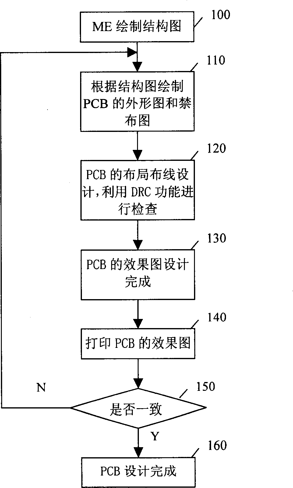
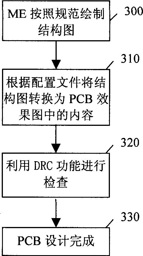
[0045] If the structure diagram drawn by ME can be directly recognized by the PCB design tool, that is, the PCB design tool can directly convert the structure diagram into a PCB design diagram, then the PCB design process can be simplified, human errors in the PCB design process can be avoided, and the PCB design process can be improved. Design efficiency and reduce PCB design cost.

[0046] Therefore, the core of the present invention is to: determine the layer specification in the structure diagram, determine the corresponding relationship between each standard layer in the structure diagram and each layer in the PCB design diagram, and when PCB design is required, according to the structure diagram Draw the corresponding structure diagram according to the layer specification, and convert the drawn structure diagram into a PCB design diagram according to the corresponding relationship.

[0047] The technical solution provided by the present invention will be further describe...


PUM


Abstract

The invention provides a method and apparatus for achieving PCB design. The method comprises: ascertaining the layer norm of the structure picture, ascertaining the corresponding relation between each norm layer and each layer of the PCB design picture, when it needs to dose PCB design, drawing the corresponding structure picture by the layer norm of the structure picture and transferring the structure picture into the PCB design picture.

Description

technical field [0001] The invention relates to the field of PCB design, in particular to a method and device for realizing PCB design. Background technique [0002] Electronic products usually put PCB (printed circuit board) in a certain shell for reasons such as mechanical environmental protection and appearance effect, which will limit the shape and size of PCB, and the mutual cooperation between PCBs will also be difficult. There are certain requirements for the position of the components on it, therefore, PCB design is very necessary. [0003] For relatively simple PCB design or small enterprises, PCB design can be carried out by manually drawing PCB illustrations. For relatively complex PCB design or large enterprises with professional ME (mechanical engineer) for detailed division of labor, in order to clearly describe the above restrictions and requirements, it is necessary to draw its structure diagram for the circuit board, and then use PCB design tools to carry o...

Claims


Application Information

Patent Timeline
Patent Type & Authority Applications(China)
IPC IPC(8): G06F17/50
Inventor 唐艳梅胡庆虎刘卫东
Owner HUAWEI TECH CO LTD
Why Eureka
Try Eureka