
Power supply processing interface in passive radio frequency identification system
A power processing, radio frequency identification technology, applied in the direction of electromagnetic radiation induction, etc., can solve the problem of weakening the induction modulation distance and so on
- Summary
- Abstract
- Description
- Claims
- Application Information
AI Technical Summary
Problems solved by technology
Method used
Image

Examples
Embodiment Construction
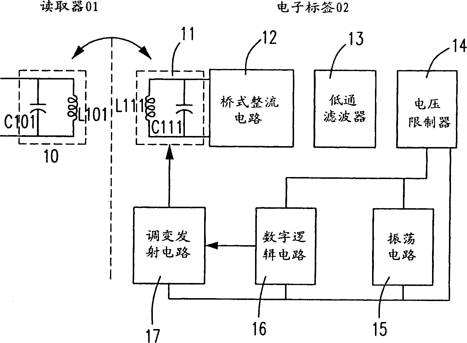
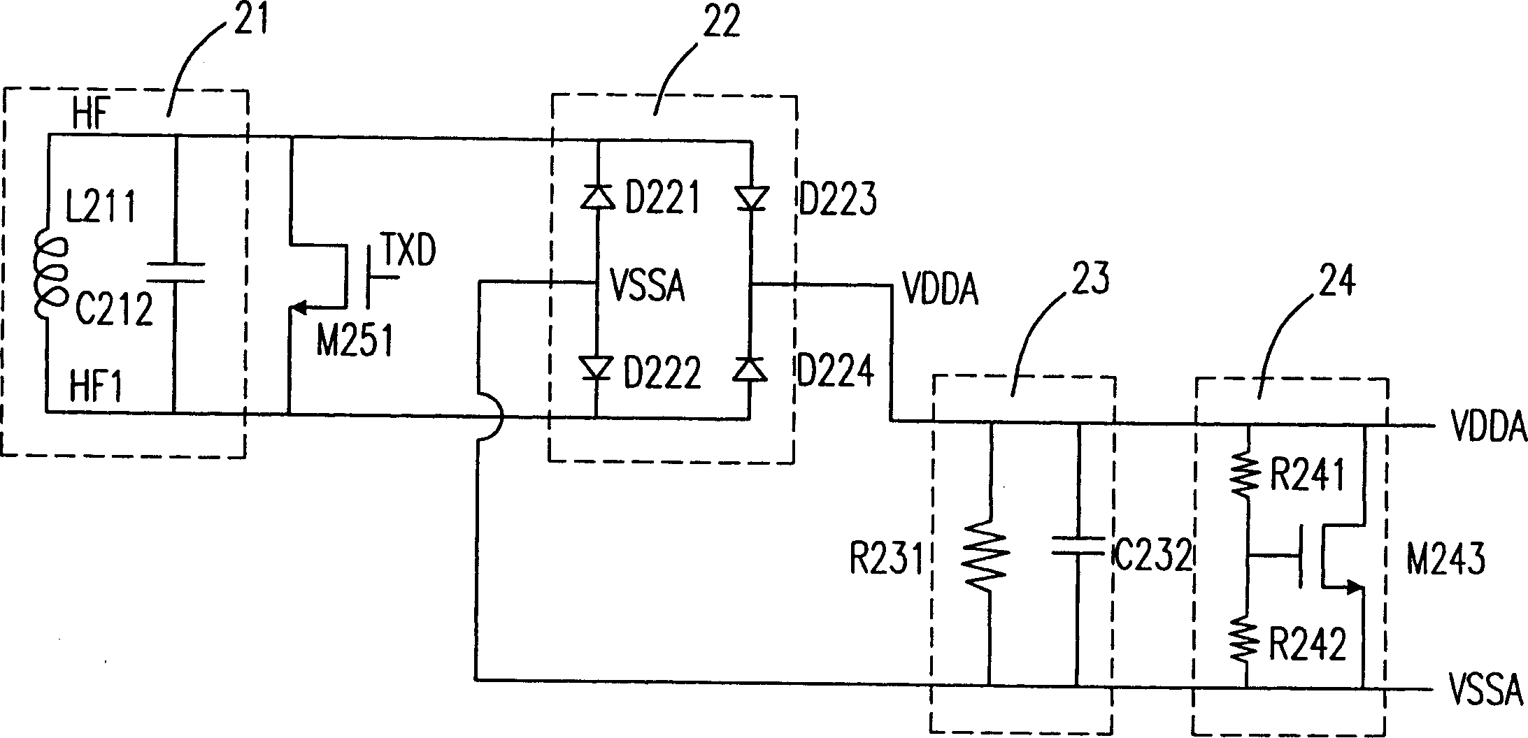
[0040] The design purpose of the present invention is to provide a stable working power supply at the tag end of the passive RFID during the AM data modulation and demodulation process of the passive RFID. Figure 4 In the conventional system architecture shown, the overvoltage detection function of the original voltage limiter 24 is separated from the voltage limiting function, and the position of the overvoltage detecting elements R241 and R242 is still maintained to detect the voltage of VDDA, but the voltage limiting element M243 is moved to the front of the bridge rectifier circuit 22. By detecting the voltage change of the output VDDA of the bridge rectifier circuit 22, the peak voltages of HF and HF1 on the LC resonant circuit 21 can be directly controlled to form an effective closed-loop device.
[0041] see Figure 5 , which is a system architecture diagram of a passive RFID tag in a preferred embodiment of the present invention. Such as Figure 5 As shown, in addit...
PUM
 Abstract
Description
Claims
Application Information