
Methods and systems for improving microelectronic

A technology for packaging components and semiconductors, which is applied in the direction of semiconductor devices, semiconductor/solid-state device manufacturing, semiconductor/solid-state device components, etc., and can solve problems such as not meeting the current demand

Inactive Publication Date: 2006-09-20
INT BUSINESS MASCH CORP
View PDF0 Cites 1 Cited by
  • Summary
  • Abstract
  • Description
  • Claims
  • Application Information

AI Technical Summary

Problems solved by technology

Therefore, the limitations of existing technical solutions will not meet the increased current demand of next-generation chip technology

Method used


Image

  • Methods and systems for improving microelectronic
  • Methods and systems for improving microelectronic
  • Methods and systems for improving microelectronic

Examples


Embodiment Construction

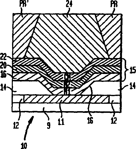
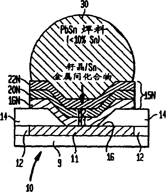
[0026] figure 1 with 2 Description is used to form one or more C4 solder bumps 24 above the metal contact 11 formed on the semiconductor device 10 on the formed conformal seed layer 15 and form one or more C4 solder balls 30 therefrom. There are technical processes. The seed layer 15 is composed of at least one bottom layer of a metal bonding layer 16. Such as figure 1 with 2 As shown, the device 10 includes a bottom layer of two metal layers 16 and 20. In order to complete the seed stack, the metal bottom layers 16 and 20 are covered by a conductive metal (CM) layer 22 composed of copper (Cu). A part of the semiconductor device 10 is shown to illustrate an example of a C4 bump formation process sequence in which the seed stack 15 is used during processing. As will be explained below, after processing, only a part of the copper originally included in the CM layer 22 remains in the CM layer 22N as figure 2 Part of the seed layer 15 of the middle layers 16N, 20N, and 22N.

[0027...


PUM


Abstract

Disclosed are microelectronic structures based on improved design and material combinations to provide improved current capabilities per I / O. The preferred embodiment of the invention uses a combination of one or more of the following: (1) Underbump metallurgy which enhances current per I / O by increasing via diameter or by having multiple via openings under BLM; (2) Thicker underbump metallurgy, where use of good conductor metallurgies can be used with increased thickness; (3) Utilizing larger via diameter under bump metallurgy, larger solder bump diameter and / or other current enhancing features for power and / or ground via connections; and (4) Using additives in Pb-free alloys to alter microstructure to minimize migration of atoms in the solder or at intermetallic transitions.

Description

Technical field [0001] The present invention relates generally to microelectronic devices, and more specifically, the present invention relates to improving the current carrying capacity of I / O connectors of microelectronic devices. Background technique [0002] In the manufacture of semiconductor devices, the semiconductor structure is electrically connected to a chip carrier, such as a ceramic substrate or a printed wiring board. Although various processes are known for making these interconnects, one process that has been widely used is the area array interconnect introduced by IBM and called Controllable Collapse Chip Connection or C4. [0003] C4 technology was developed by IBM in the 1960s and it offers many advantages. One advantage is the high input / output density of the C4 process, which allows solder bumps to be placed anywhere on the chip, making it easier to connect to the circuit at those connection points. In addition, short solder bumps improve overall electrical p...

Claims


Application Information

Patent Timeline
Patent Type & Authority Applications(China)
IPC IPC(8): H01L23/48H01L21/60
CPCH01L2924/01051H01L2924/01027H01L2924/01002H01L2924/0105H01L2924/01025H01L2924/01327H01L2924/01076H01L2924/01059H01L2924/01078H01L2924/01028H01L2924/14H01L2924/01014H01L24/10H01L24/02H01L24/13H01L2924/01082H01L2224/13099H01L2924/01022H01L2924/01322H01L2924/0104H01L2924/014H01L2224/0401H01L2924/01029H01L2924/01012H01L2924/01019H01L2924/01033H01L2924/15787H01L2224/13H01L24/03H01L24/05H01L24/11H01L2924/00
Inventor 约翰·U·克尼克伯克海·P·郎沃斯罗格·A·居昂
Owner INT BUSINESS MASCH CORP
Learn More