Chemical solution for electroplating a copper-zinc alloy thin film

Inactive Publication Date: 2005-12-13
ADVANCED MICRO DEVICES INC
View PDF22 Cites 19 Cited by
  • Summary
  • Abstract
  • Description
  • Claims
  • Application Information

AI Technical Summary

Benefits of technology

[0013]By electroplating this Cu—Zn alloy thin film on the Cu surface using a stable chemical solution in the prescribed concentration ranges, the present invention improves Cu interconnect reliability, enhances electromigration resistance, improves corrosion resistance, and reduces manufacturing costs. In particular, the present invention chemical solution is advantageous in that it facilitates formation of an acceptable Cu—Zn alloy thin film over a wide range of bath compositions. The desirable Zn concentration in the Cu—Zn alloy thin film, preferably in a range of approximately 0.2 at. % to approximately 9.0 at. % determined by X-Ray Photoelectron Spectroscopy (XPS) or Auger Electron Spectroscopy (AES), is controllable by varying the electroplating conditions and/or the bath composition.
[0014]These advantages arise from the present invention's superior fill-characteristics. The present Cu—Zn electroplating solution facilitates better filling of a Cu—Zn alloy thin film on an interconnect, especially for feature sizes in a dimensional range of approximately 0.2 μΩ.cm to approximately 0.05 μm, thereby lowering the resistance of the formed Cu—Zn alloy thin film (e.g., in a resistance range of approximately 2.2 μΩ.cm to approximately 2.5 μΩ.cm for approximately 1

Problems solved by technology

Despite aluminum's (Al) adequate resistance, other Al properties render it less desirable as a candidate for these higher density devices, especially with respect to its deposition into plug regions having a high aspect ratio cross-sectional area.
However, some disadvantages of using Cu as an interconnect material include etching problems, corrosion, and diffusion into silicon.1 These proble

Method used


Image

  • Chemical solution for electroplating a copper-zinc alloy thin film
  • Chemical solution for electroplating a copper-zinc alloy thin film
  • Chemical solution for electroplating a copper-zinc alloy thin film

Examples


Example

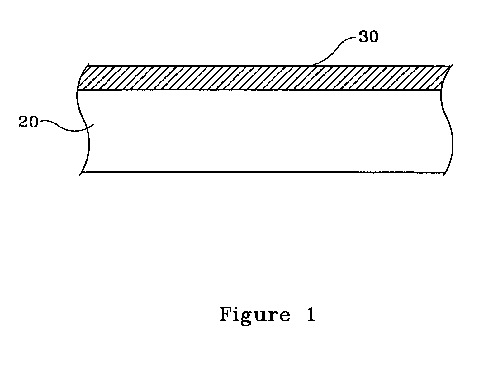
[0019]FIG. 1 illustrates, by example only, and in cross-section, a Cu surface 20 having a Cu—Zn alloy thin film 30 thereon deposited, in accordance with the present invention.

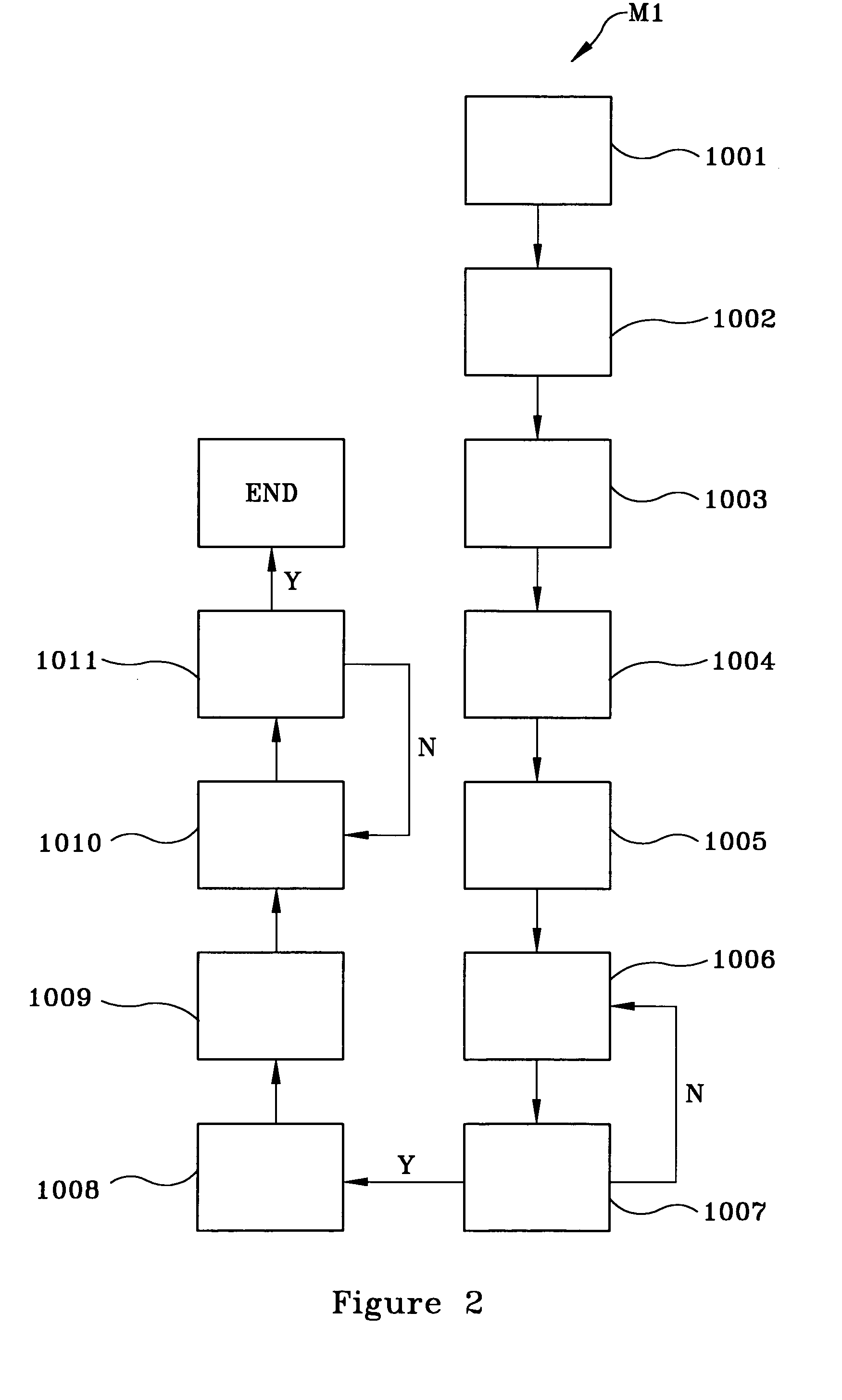
[0020]FIG. 2 flowcharts, by example only, a method M1 for synthesizing a liter of a unique nontoxic aqueous Cu—Zn electroplating (chemical) solution, in accordance with the present invention:[0021](1) cleaning a mixing vessel (e.g., a beaker) with dilute nitric acid (HNO3) for approximately 5 minutes, as indicated by block 1001;[0022](2) rinsing the mixing vessel in deionized (DI) water for approximately 5 minutes to approximately 10 minutes and subsequently drying the mixing vessel, for instance, under a gaseous nitrogen (GN2) flow, as indicated by block 1002;[0023](3) adding an initial volume of DI water (e.g., approximately 400 ml) to the mixing vessel, as indicated by block 1003;[0024](4) adding at least one Cu ion source for providing a plurality of Cu ions and stirring the at least one Cu ion source into ...


PUM

PropertyMeasurementUnit
Temperatureaaaaaaaaaa
Densityaaaaaaaaaa

Abstract

A method of fabricating a semiconductor device, having a Cu—Zn alloy thin film (30) formed on a Cu surface (20) by electroplating the Cu surface (20) in a unique chemical solution containing salts of zinc (Zn) and copper (Cu), their complexing agents, a pH adjuster, and surfactants; and a semiconductor device thereby formed. The method controls the parameters of pH, temperature, and time in order to form a uniform Cu—Zn alloy thin film (30) for reducing electromigration in Cu interconnect lines by decreasing the drift velocity therein which decreases the Cu migration rate in addition to decreasing the void formation rate, for improving Cu interconnect reliability, and for increasing corrosion resistance.

Description

CROSS-REFERENCE TO RELATED APPLICATION(S)[0001]This application is also related to the following commonly assigned applications, entitled:[0002](1) “Method of Electroplating a Copper-Zinc Alloy Thin Film on a Copper Surface Using a Chemical Solution and a Semiconductor Device thereby Formed,” concurrently filed (Ser. No. 10 / 082,432);[0003](2) “Method of Controlling Zinc-Doping in a Copper-Zinc Alloy Thin Film Electroplated on a Copper Surface and a Semiconductor Device thereby Formed,” concurrently filed (Ser. No. 10 / 082,433);[0004](3) “Method of Reducing Electromigration in a Copper Line by Electroplating an Interim Copper-Zinc Alloy Thin Film on a Copper Surface Using a Chemical Solution and a Semiconductor Device thereby Formed,” concurrently filed (Ser. No. 10 / 083,809);[0005](4) “Method of Reducing Electromigration in a Copper Line by Zinc-Doping of a Copper Surface from an Electroplated Copper-Zinc Alloy Thin Film and a Semiconductor Device thereby Formed,” filed on Dec. 7, 200...

Claims


Application Information

Patent Timeline
IPC IPC(8): C25D3/58C25D7/12H01L21/288H01L21/768
CPCC25D3/58C25D7/12H01L21/2885H01L21/76838H01L21/7685C25D7/123
Inventor LOPATIN, SERGEY
Owner ADVANCED MICRO DEVICES INC
Why Eureka
Try Eureka