Method of reducing electromigration by forming an electroplated copper-zinc interconnect and a semiconductor device thereby formed

a technology of copper-zinc alloy and interconnect, which is applied in the field of reducing electromigration by forming an electroplated copper-zinc interconnect and a semiconductor device thereby formed, can solve the problems of neither technique providing a cost-effective method of forming a copper-zinc alloy on a cu interconnect surface, and is less desirable as a candidate for these higher density devices, so as to reduce the electromigration in the device, improve the reliability and corrosion of the interconn

Inactive Publication Date: 2004-04-06
GLOBALFOUNDRIES US INC
View PDF7 Cites 16 Cited by
  • Summary
  • Abstract
  • Description
  • Claims
  • Application Information

AI Technical Summary

Benefits of technology

Accordingly, the present invention provides a method of reducing electromigration in a dual-inlaid copper interconnect line by filling a via with a Cu-rich (e.g., approximately 99.8 at.% to approximately 98 at.% / o) copper-zinc (Cu--Zn) alloy electroplated on a copper (Cu) surface from a stable chemical solution, and by controlling the Zn-doping thereof (e.g., approximately 0.2 at.% to approximately 2.0 at.%), which also improves interconnect reliability and corrosion resistance, and a semiconductor device thereby formed. The present method involves filling the via by electroplating the Cu surface, such as a blanket Cu seed layer and a partial thickness plated Cu layer, in a unique nontoxic aqueous chemical electroplating solution containing salts of zinc (Zn) and copper (Cu), their complexing agents, a pH adjuster, and surfactants, thereby forming an electroplated Cu--Zn alloy fill having some degree of oxygen (O) concentration, wherein the Zn-doping is controllable by varying the electroplating conditions; and annealing the Cu--Zn alloy fill formed on the Cu surface in an environment such as vacuum, nitrogen (N.sub.2), hydrogen (H.sub.2), forming (N.sub.2 H.sub.2), or mixtures thereof for reducing the O-concentration in the alloy fill, for modifying the grain structure of the Cu--Zn alloy fill as well as of the underlying Cu surface, and for forming a mixed Cu--Zn / Cu interface, thereby forming the dual-inlaid interconnect structure. The present invention further provides a particular electroplating method which controls the parameters of Zn concentration, pH, temperature, and time in order to form a uniform reduced-oxygen copper-zinc (Cu--Zn) alloy fill on a cathode-wafer surface such as a copper (Cu) surface for reducing electromigration in the device by deceasing the drift velocity therein which decreases the Cu migration rate in addition to decreasing the void formation rate.
More specifically, the present invention provides a method of fabricating a semiconductor device, having a reduced-oxygen copper-zinc (Cu--Zn) alloy fill formed on a copper (Cu) surface by electroplating the Cu surface in a chemical solution, generally comprising the steps of: providing a semiconductor substrate having a Cu surface (e.g., seed layer), the Cu surface having been formed by CVD, PVD, PECVD, ALD, or electroplating, an optional barrier layer, and an optional underlayer formed in a via; providing a chemical solution; immersing the Cu surface in the chemical solution, thereby forming a Cu--Zn alloy fill on the Cu surface in the via; rinsing the Cu--Zn alloy fill in a solvent; drying the Cu--Zn alloy fill under a gaseous flow; annealing the Cu--Zn alloy fill formed on the Cu surface, thereby forming a reduced-oxygen Cu--Zn alloy fill; planarizing the reduced-oxygen Cu--Zn alloy fill, the Cu surface, the optional barrier layer, and the optional underlayer, thereby forming a Cu--Zn alloy dual-inlaid interconnect structure; and completing formation of the semiconductor device.
By electroplating this Cu--Zn alloy fill in the via and on the cathode-wafer surface, such as a Cu surface, using a stable chemical solution in the prescribed concentration ranges and subsequently annealing the Cu--Zn alloy fill electroplated on the Cu surface, the present invention improves Cu interconnect reliability, enhances electromigration resistance, improves corrosion resistance, and reduces manufacturing costs. In particular, the present invention chemical solution is advantageous in that it facilitates formation of an acceptable Cu--Zn alloy fill over a wide range of bath compositions while the subsequent annealing step removes undesirable oxygen impurities from the formed alloy fill. The desirable Zn concentration in the Cu--Zn alloy fill, preferably in a range of approximately 0.2 at% to approximately 2.0 at% determined by X-Ray Photoelectron Spectroscopy (XPS) or Auger Electron Spectroscopy (AES), is controllable by varying the electroplating conditions and / or the bath composition. By so controlling the Zn-doping, the present method balances high electromigration performance against low resistively requirements. Additionally, the Cu surface (e.g., seed layer), being formed by a technique such as electroless deposition, ion metal plasma (IMT), self-ionized plasma (SIP), hollow cathode magnetron (HCM), chemical vapor deposition (CVD), and atomic layer deposition (ALD), is enhanced by the Cu--Zn alloy fill layer and is prevented from etching by the high pH value (i.e., basic) of the chemical solution from which the alloy fill layer is formed.
Further advantages arise from the present invention's superior fill-characteristics. The present Cu--Zn electroplating solution facilitates better filling of the via on an interconnect, especially for feature sizes in a dimensional range of approximately 0.2 .mu.m to approximately 0.05 .mu.m, thereby lowering the resistance of the formed Cu--Zn alloy fill (e.g., in a resistance range of approximately 2.2 .mu..OMEGA..multidot.cm to approximately 2.5 .mu..OMEGA..multidot.cm for approximately 1 at.% Zn content in a Cu--Zn alloy fill, as deposited). Further, the filling capability is enhanced by three beneficial characteristics of the present invention: (1) the instant chemical solution does not etch copper or a copper alloy seed layer; (2) the introduction of Zn into the alloy fill as well as onto the Cu interconnect improves both step coverage and nucleation; and (3) a variety of organic additives, such as polyethylene glycol (PEG), organo-disulfides, and organo-chlorides, are compatible and may be included in the instant chemical solution for further enhancing the fill profile and grain structure. The present Cu--Zn electroplating solution provides a desirably low Zn content in a Cu alloy interconnect (e.g., in a concentration range of approximately 0.2 at.% to approximately 1.0 at%) which also imparts (1) a de minimis increase in resistance as well as (2) a maximum improvement in electromigration resistance. The present chemical solution can also provide a desirably low Zn content (e.g., in a range of <<approximately 0.1 at.% or <<approximately 0.2 at %, virtually undetectable by AES) in a Cu film, wherein the Zn content may be engineered by varying the deposition parameters as well as by modifying the bath composition.

Problems solved by technology

Despite aluminum's (Al) adequate resistance, other Al properties render it less desirable as a candidate for these higher density devices, especially with respect to its deposition into plug regions having a high aspect ratio cross-sectional area.
However, some disadvantages of using Cu as an interconnect material include etching problems, corrosion, and diffusion into silicon..sup.1 These problems have instigated further research into the formulation of barrier materials for preventing electromigration in both Al and Cu interconnect lines.
Further, though CVD and PECVD have been conventionally used for depositing secondary metal(s) on a primary metal interconnect surface, neither technique provides a cost-effective method of forming a copper-zinc alloy on a Cu interconnect surface.

Method used


Image

  • Method of reducing electromigration by forming an electroplated copper-zinc interconnect and a semiconductor device thereby formed
  • Method of reducing electromigration by forming an electroplated copper-zinc interconnect and a semiconductor device thereby formed
  • Method of reducing electromigration by forming an electroplated copper-zinc interconnect and a semiconductor device thereby formed

Examples


Embodiment Construction

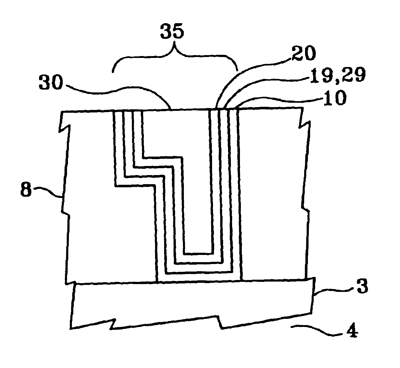
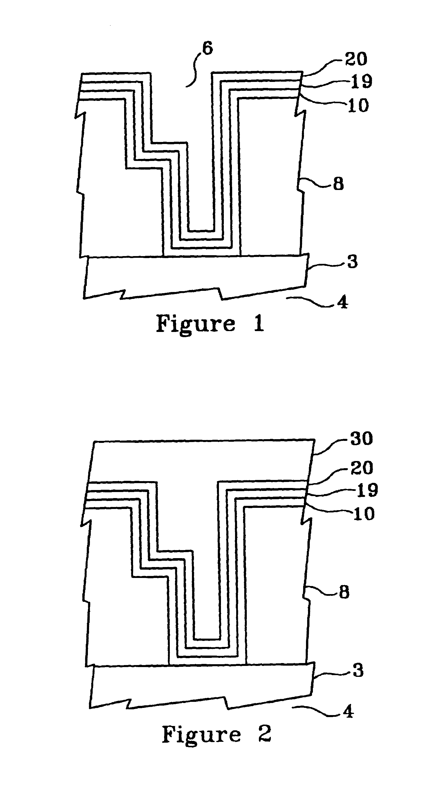
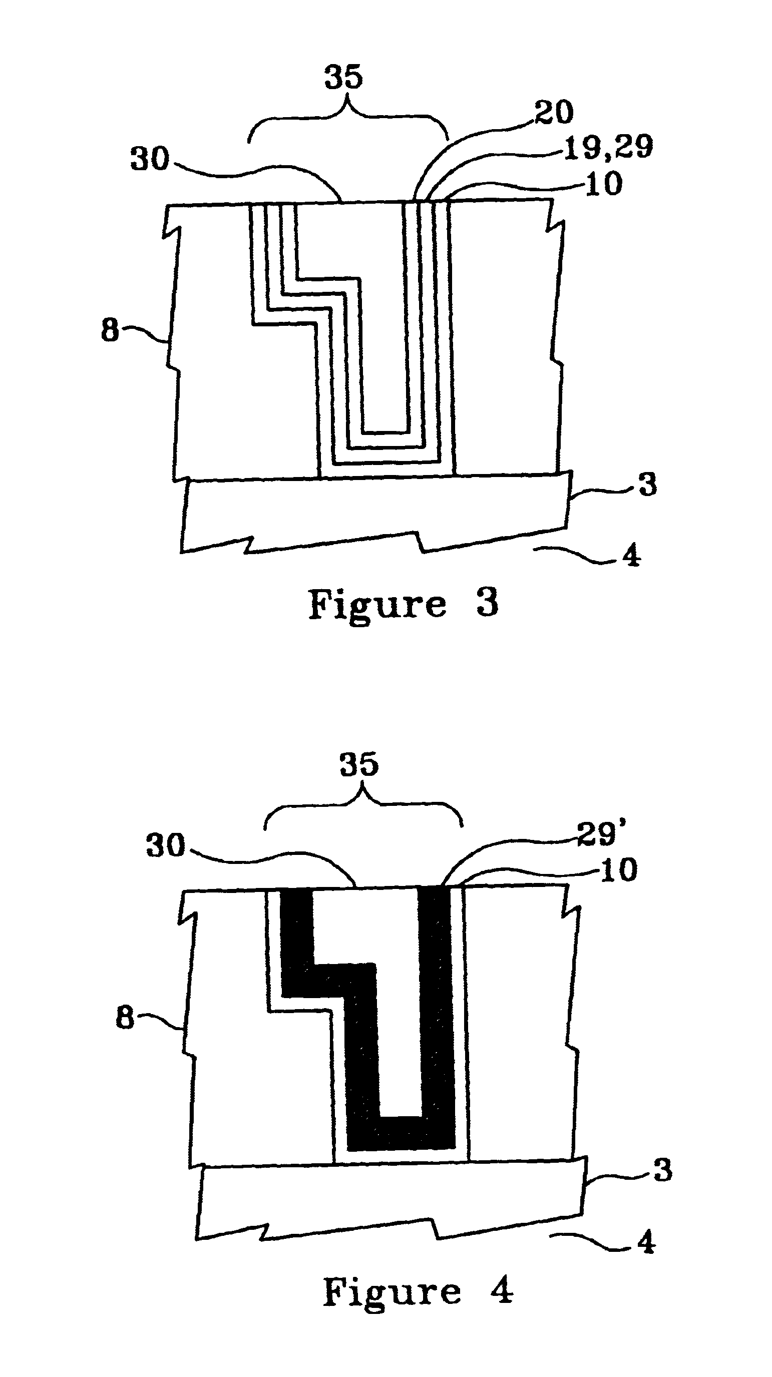
FIG. 1 illustrates, by example only, in cross-section, a Cu interconnect line 3 formed on a semiconductor substrate 4 and acting as the bottom portion of a via 6, the via 6 sidewalls comprising at least one low dielectric constant layer 8, in a dielectric constant range of approximately 1.6 to approximately 2.3, the via 6 having an optional barrier layer 10 formed by a technique such as chemical vapor deposition (CVD) or atomic layer deposition (ALD), comprising at least one material selected from a group consisting essentially of titanium silicon nitride (Ti.sub.x Si.sub.y N.sub.2), tantalum nitride (TaN), and tungsten nitride (W.sub.x N.sub.y) in a thickness range of approximately 30 .ANG. to approximately 50 .ANG., formed therein, an optional underlayer 19, comprising at least one material selected from a group consisting essentially of tin (Sn) and palladium Ed) and having a thickness of range of approximately 15 .ANG. to approximately 50 .ANG.(preferably approximately 30 .ANG.)...


PUM

PropertyMeasurementUnit
thicknessaaaaaaaaaa
thicknessaaaaaaaaaa
thicknessaaaaaaaaaa

Abstract

A method of reducing electromigration in a dual-inlaid copper interconnect line (3) by filling a via (6) with a Cu-rich Cu-Zn alloy (30) electroplated on a Cu surface (200 from a stable chemical solution, and by controlling the Zn-doping thereof, which also improves interconnect reliability and corrosion resistance, and a semiconductor device thereby formed. The method involves using a reduced-oxygen Cu-Zn alloy as fill (30) for the via (6) in forming the dual-inlaid interconnect structure (35). The alloy fill (30) is formed by electroplating the Cu surface (20) in a unique chemical solution containing salts of Zn and Cu, their complexing agents, a pH adjuster, and surfactants, thereby electroplating the fill (30) on the Cu surface (20); and annealing the electroplated Cu-Zn alloy fill (30); and planarizing the Cu-Zn alloy fill (30), thereby forming the dual-inlaid copper interconnect line (35).

Description

FIELD OF THE INVETIONThe present invention relates to semiconductor devices and their methods of fabrication. More particularly, the present invention relates to the processing of copper interconnect material and the resultant device utilizing the same. Even more particularly, the present invention relates to reducing electromigration in copper interconnect lines by doping their surfaces with a barrier material using wet chemical methods.Currently, the semiconductor industry is demanding faster and denser devices (e.g., 0.05-.mu.m to 0.25-.mu.m) which implies an ongoing need for low resistance metallization. Such need has sparked research into resistance reduction through the use of barrier metals, stacks, and refractory metals. Despite aluminum's (Al) adequate resistance, other Al properties render it less desirable as a candidate for these higher density devices, especially with respect to its deposition into plug regions having a high aspect ratio cross-sectional area. Thus, rese...

Claims


Application Information

Patent Timeline
Patent Type & Authority Patents(United States)
IPC IPC(8): H01L21/02H01L21/4763H01L27/102H01L27/082C25D3/58C25D7/12H01L21/288H01L21/768
CPCC25D3/58H01L21/2885H01L21/76877C25D7/123C25D17/001
Inventor LOPATIN, SERGEYNICKEL, ALEXANDER H.KING, PAUL L.
Owner GLOBALFOUNDRIES US INC
Why Eureka
Try Eureka