
Multiple copper vias for integrated circuit metallization and methods of fabricating same

a technology of integrated circuits and copper vias, which is applied in the direction of semiconductor/solid-state device testing/measurement, semiconductor devices, semiconductor/solid-state device details, etc., can solve the problems of affecting the reliability of metal-based interconnects for integrated circuits, affecting the quality and/or reliability of high-density microelectronic devices, and accumulation of vacancies or voids in conductors. , to achieve the effect of reducing the driving force of electromig

Inactive Publication Date: 2005-07-19
BOARD OF RGT THE UNIV OF TEXAS SYST
View PDF15 Cites 18 Cited by
  • Summary
  • Abstract
  • Description
  • Claims
  • Application Information

AI Technical Summary

Benefits of technology

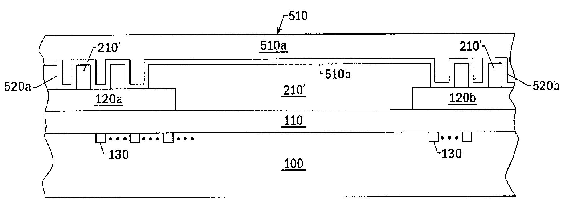
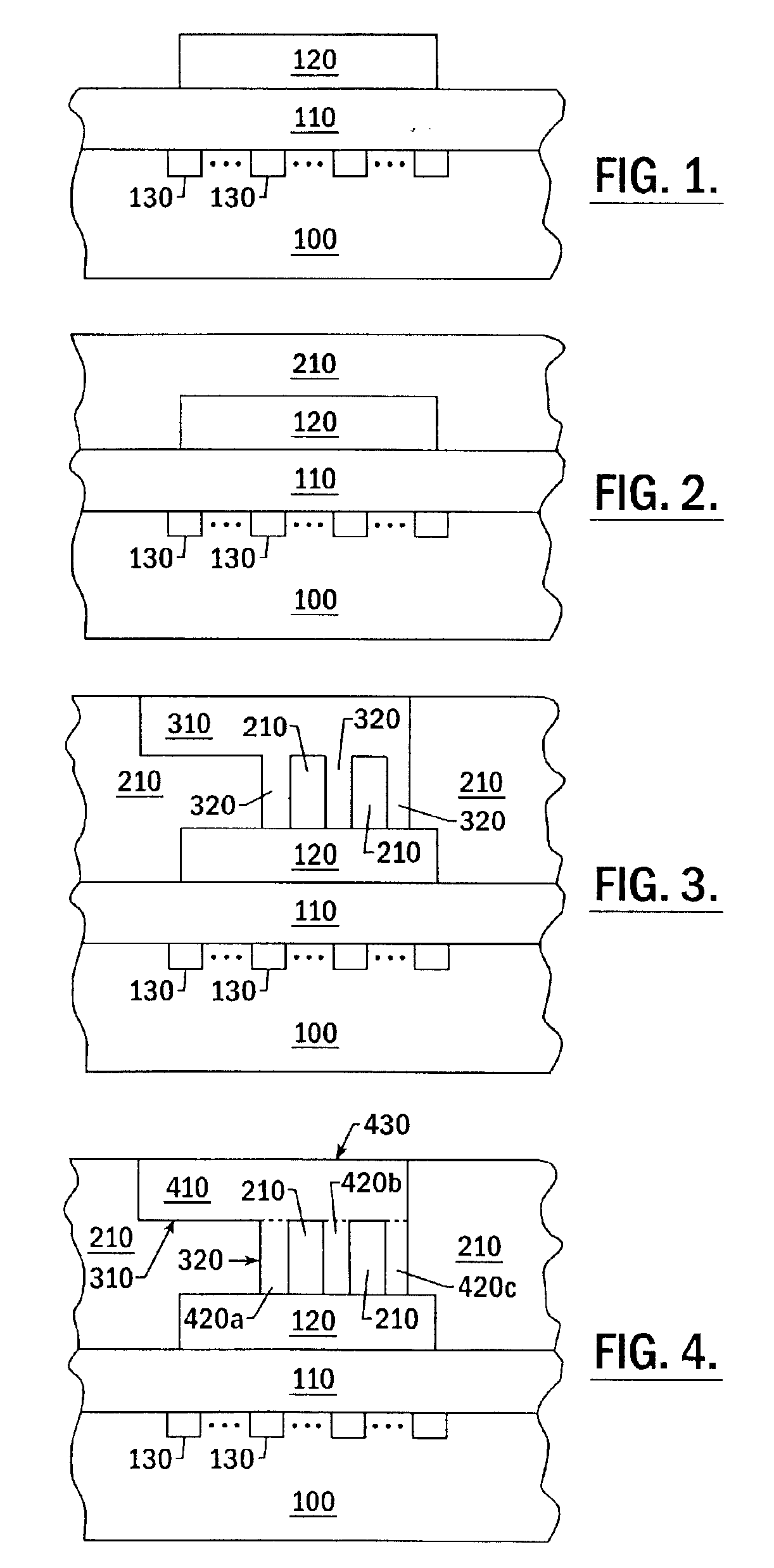
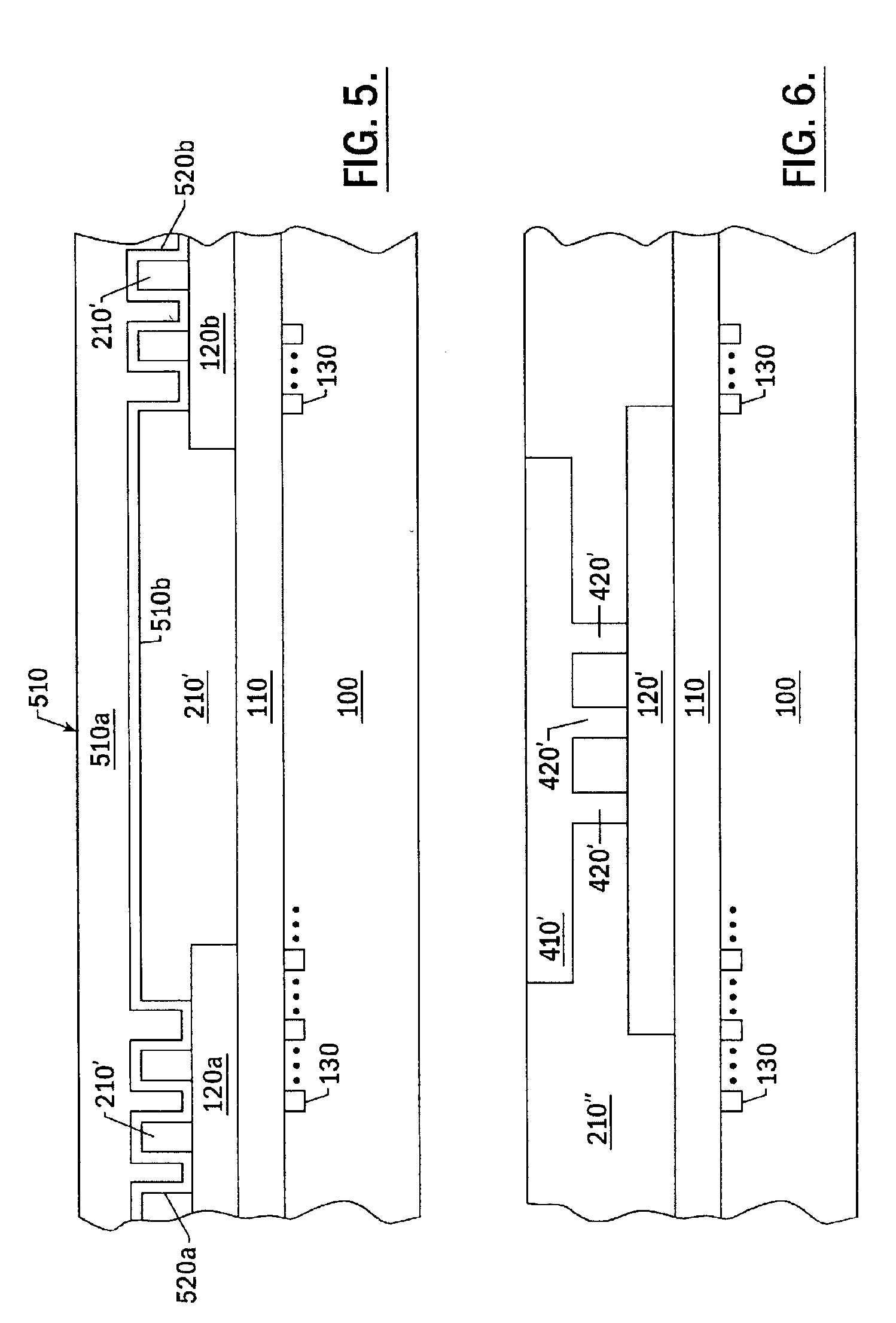
[0010]Some embodiments of the present invention can reduce electromigration in a copper-based metallization of an integrated circuit that includes a first copper-containing via (i.e., a via comprising copper) that electrically connects an underlying conductive line and an overlying copper-containing line through an intervening insulating layer. According to some embodiments of the invention, at least a second copper-containing via is formed that electrically connects the underlying conductive line and the overlying copper-containing line through the intervening insulating layer, in parallel with the first copper-containing via. Without wishing to be bound by any theory of operation, it has been found, according to some embodiments of the present invention, that multi-vias can provide redundancy to improve early failure statistics. Moreover, since current is distributed among the multi-vias, the electromigration driving force can be reduced and local Joule heating in voids at the via interface, also may be reduced. Accordingly, even if via voids are formed, the structure may not fail by catastrophic thermal runaway due to Joule heating.

Problems solved by technology

As the integration density of integrated circuit devices continues to increase, it may be difficult to form interconnections among these high density microelectronic devices with sufficient quality and / or reliability.
It is well known that electromigration can impact the reliability of metal-based interconnects for integrated circuits.
A divergence of ionic flux can lead to an accumulation of vacancies or voids in the conductor.
These voids may grow to be a large enough size so as to cause an open circuit failure of the conductor.
Statistical studies have revealed multi-mode failures in copper-based dual-damascene structures, one mode of failure due to void formation at the via interface and other modes comprising void formation in the line or metal extrusion near the end of the metal line.
Void formation at the via interface usually occurs faster than other failure modes, therefore it dominates the early failures of copper interconnects.
Early failures may be a significant concern, since they may dominate the lifetime of the integrated circuit as the device scaling results in increasing interconnect density.
Electromigration failure at the via may be caused by flux divergence occurring at the via / line interface due to the presence of a diffusion barrier and due to the via geometry.

Method used


Image

  • Multiple copper vias for integrated circuit metallization and methods of fabricating same
  • Multiple copper vias for integrated circuit metallization and methods of fabricating same
  • Multiple copper vias for integrated circuit metallization and methods of fabricating same

Examples


Embodiment Construction

[0025]The present invention now will be described more fully hereinafter with reference to the accompanying figures, in which embodiments of the invention are shown. This invention, however, should not be construed as limited to the embodiments set forth herein.

[0026]Accordingly, while the invention is susceptible to various modifications, specific embodiments thereof are shown by way of example in the drawings and will herein be described in detail. It should be understood, however, that there is no intent to limit the invention to the particular forms disclosed, but on the contrary, the invention is to cover all modifications, equivalents, and alternatives falling within the spirit and scope of the invention as defined by the claims.

[0027]Like numbers refer to like elements throughout the description of the figures. In the figures, the dimensions of layers and regions may be exaggerated for clarity. It will also be understood that when an element, such as a layer, region or substr...


PUM


Abstract

Electromigration can be reduced in a copper-based metallization of an integrated circuit that includes a first copper-containing via that electrically connects an underlying conductive line and an overlying copper-containing line through an intervening insulating layer. Electromigration can be reduced by forming at least a second copper-containing via that electrically connects the underlying conductive line and the overlying copper-containing line through the intervening insulating layer, in parallel with the first copper-containing via. Multi-vias can provide redundancy to reduce early failure statistics. Moreover, since current is distributed among the vias, the electromigration driving force can be reduced and local Joule heating, in voids at the via interface, also may be reduced. Accordingly, even if via voids are formed, the structure may not fail by catastrophic thermal runaway due to Joule heating.

Description

FIELD OF THE INVENTION[0001]This invention relates to integrated circuits and fabrication methods therefor, and more specifically to copper-based interconnect metallization for integrated circuits and fabrication methods therefor.BACKGROUND OF THE INVENTION[0002]Integrated circuits are widely used in consumer, commercial and industrial applications. As is well known to those having skill in the art, an integrated circuit may comprise an integrated circuit substrate, such as a silicon semiconductor substrate including a plurality of a microelectronic devices therein, and an interconnect system on the integrated circuit substrate for selectively interconnecting the microelectronic devices and / or for providing power supply and / or input / output connections. As the integration density of integrated circuit devices continues to increase, it may be difficult to form interconnections among these high density microelectronic devices with sufficient quality and / or reliability.[0003]Copper is b...

Claims


Application Information

Patent Timeline
Patent Type & Authority Patents(United States)
IPC IPC(8): H01L23/52H01L23/522H01L23/532H01L23/544
CPCH01L22/34H01L23/522H01L23/53228H01L23/5226H01L2924/0002H01L2924/00
Inventor HO, PAUL S.LEE, KI-DONOGAWA, ENNISMATSUHASHI, HIDEKI
Owner BOARD OF RGT THE UNIV OF TEXAS SYST
Learn More