Reduced electromigration and stressed induced migration of copper wires by surface coating

a technology of stress-induced migration and surface coating, applied in the direction of liquid/solution decomposition chemical coating, semiconductor/solid-state device details, coatings, etc., can solve the problem that the specifications of allowed current in cu conductors are not significantly superior to those for al(cu), and the cu conductor pattern is susceptible to atomic voiding, so as to reduce the susceptibility to electromigration, improve reliability and yield, and reduce the effect of susceptibility to stress-induced migration

Inactive Publication Date: 2005-12-01
GLOBALFOUNDRIES INC
View PDF20 Cites 18 Cited by
  • Summary
  • Abstract
  • Description
  • Claims
  • Application Information

AI Technical Summary

Benefits of technology

[0005] In accordance with the present invention, the exposed Cu surface of a Cu conductor is altered by providing a thin metal layer in the range from 1 to 20 nm on the Cu surface, such as subsequent to a CMP planarization or a dry etching process, in order to reduce susceptibility to electromigration, oxidation, corrosion, stress voiding and delamination during subsequent chip processing and / or chip utilization, thus improving reliability and yield. This invention teaches the method of electroless metal deposition as one way to form a thin metal layer on a Cu conductor to increase electromigration lifetime and stress induced migration resistance.

Problems solved by technology

At the same time, the need for higher levels of current density has exposed the Al(Cu) lines to failure by electromigration, limiting the extent to which circuit designers can increase performance.
Thus, the specifications for allowed current in Cu conductors proved not to be significantly superior to those for Al(Cu).
In addition to electromigration lifetime failure, it was found that Cu conductor patterns are susceptible to atomic voiding under thermal cycle stress, with voids always found to be initiated at the Cu / dielectric interface where the atomic mobility is highest.

Method used


Image

  • Reduced electromigration and stressed induced migration of copper wires by surface coating
  • Reduced electromigration and stressed induced migration of copper wires by surface coating
  • Reduced electromigration and stressed induced migration of copper wires by surface coating

Examples


Embodiment Construction

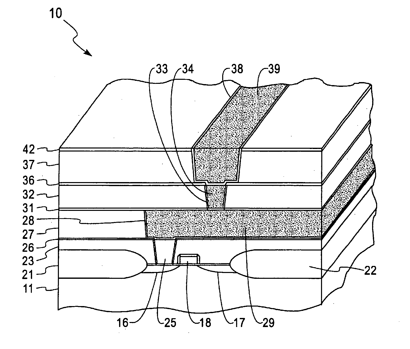
[0024] Referring now to the drawing, FIG. 1 is a cross section view of an example of a Cu Back End of the Line (BEOL) structure on an integrated circuit chip 10 containing Cu lines and vias produced by a single damascene process.

[0025] In FIG. 1, integrated circuit chip 10 has a substrate 11 which may be, for example, Si, SiGe, Ge, SOI and GaAs. Substrate 11 may have formed therein, source 16 and drain 17 regions and gate 18 of a typical FET transistor 19. On either side of source 16 and drain 17 regions are recessed oxide regions 21 and 22 on substrate 11. A layer 23 of oxide is formed over oxide regions 21 and 22 and FET transistor 19. A source contact opening is formed layer 23 and filled with metal 25 which is usually tungsten. Layer 23 and metal 25 are planarized by Chemical Mechanical Polishing (CMP). A capping layer 26 of, for example, silicon nitride is formed on the upper surface of layer 23. Layer 27 of dielectric is formed on layer 26 and trenches are formed therein. A l...


PUM

PropertyMeasurementUnit
thicknessaaaaaaaaaa
thicknessaaaaaaaaaa
temperatureaaaaaaaaaa

Abstract

The idea of the invention is to coat the free surface of patterned Cu conducting lines in on-chip interconnections (BEOL) wiring by a 1-20 nm thick metal layer prior to deposition of the interlevel dielectric. This coating is sufficiently thin so as to obviate the need for additional planarization by polishing, while providing protection against oxidation and surface, or interface, diffusion of Cu which has been identified by the inventors as the leading contributor to metal line failure by electromigration and thermal stress voiding. Also, the metal layer increases the adhesion strength between the Cu and dielectric so as to further increase lifetime and facilitate process yield. The free surface is a direct result of the CMP (chemical mechanical polishing) in a damascene process or in a dry etching process by which Cu wiring is patterned. It is proposed that the metal capping layer be deposited by a selective process onto the Cu to minimize further processing. We have used electroless metal coatings, such as CoWP, CoSnP and Pd, to illustrate significant reliability benefits, although chemical vapor deposition (CVD) of metals or metal forming compounds can be employed.

Description

FIELD OF THE INVENTION [0001] This invention relates to metal interconnections on semiconductor chips and more particularly to a surface coating or treatment to prevent surface atoms of conductors from being moved downstream by an electron current, a phenomena known as electromigration, and / or from being moved by a stress gradient tending to relax stress known as stress induced migration. BACKGROUND OF THE INVENTION [0002] Increased density and speed of microelectronic circuitry has caused a shift in the metallization system from Al(Cu) to Cu to reduce the resistance of the conductor. At the same time, the need for higher levels of current density has exposed the Al(Cu) lines to failure by electromigration, limiting the extent to which circuit designers can increase performance. The higher melting point of Cu is expected to improve the current carrying capability of the conductors, extending electromigration lifetime. However, from our test results, we have found that the electromig...

Claims


Application Information

Patent Timeline
Patent Type & Authority Applications(United States)
IPC IPC(8): H01L21/28H01L21/288C23C18/16H01L21/3205H01L21/44H01L21/4763H01L21/768H01L23/52H01L23/532
CPCH01L21/288H01L21/76843H01L21/76849H01L21/76864H01L23/53228H01L2924/0002H01L23/53238H01L23/5329H01L2924/00H01L21/3205B82Y40/00
Inventor HU, CHAO-KUNROSENBERG, ROBERTRUBINO, JUDITH MARIESAMBUCETTI, CARLOS JUANSTAMPER, ANTHONY KENDALL
Owner GLOBALFOUNDRIES INC
Why Eureka
Try Eureka