Inductive coupling plasma device

An inductive coupling, plasma technology, applied in the direction of plasma, circuits, electrical components, etc., can solve the problems of plasma density asymmetry, uneven wafer etching rate, unstable semiconductor processing quality, etc., to achieve the etching rate The effect of uniformity, small speed difference and improved quality

Active Publication Date: 2006-10-18
BEIJING NAURA MICROELECTRONICS EQUIP CO LTD
View PDF0 Cites 9 Cited by
  • Summary
  • Abstract
  • Description
  • Claims
  • Application Information

AI Technical Summary

Problems solved by technology

Especially after the processing size of the wafer 5 increases from 100 mm to 300 mm, and the volume of the reaction chamber 3 increases accordingly, the plasma density excited by the planar inductively coupled coil 4 has a large asymmetry in azimuth angle, so it can only rely on Diffusion to compensate for peripheral low-density regions
As a result, the etching rate of the wafer is not uniform, the quality of semiconductor processing is unstable, and the product use effect is affected.

Method used


Image

  • Inductive coupling plasma device
  • Inductive coupling plasma device

Examples


Embodiment Construction

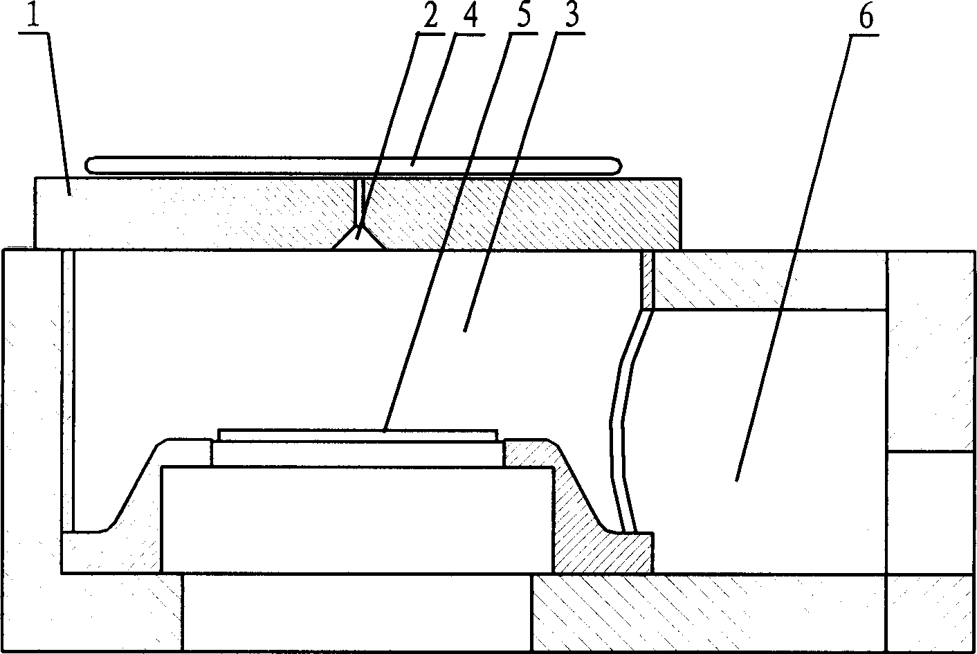
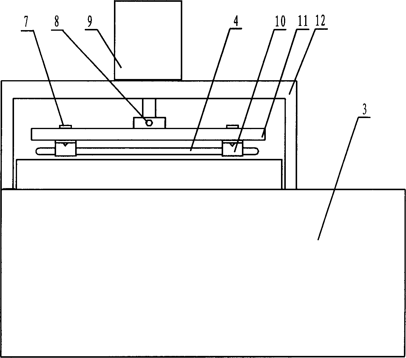
[0011] The specific embodiment of the inductively coupled plasma device described in the present invention is as follows figure 2 Shown: includes an inductively coupled plasma cavity, an inductively coupled coil 4 and a coil rotating device. The inductively coupled coil 4 is located above the inductively coupled plasma cavity. The inductively coupled coil 4 is installed on the coil rotating device, and the input and output terminals of the inductively coupled coil 4 are connected to the power supply through brushes. The rotating device is fixed on the inductively coupled plasma cavity. The coil rotating device includes a motor 9 , a fixed disk 11 and a bracket 12 . The bracket 12 is fixed on the inductively coupled plasma cavity, and the shaft end of the motor 9 is installed downward on the beam of the bracket 12. The 9 shafts of the motor are connected with the center hole of the fixed disk 11 and fixed with screws 8. The inductively coupled coil 4 passes through the clamp ...


PUM


Abstract

The present invention relates to an inductively-coupled plasma device, including inductively-coupled plasma cavity body, inductively-coupled coil and coil rotating device. The inductively-coupled coil is positioned over the inductively-coupled plasma cavity body, the inductively-coupled coil is mounted on the coil rotating device, the coil rotating device is fixed on the inductively-coupled plasma cavity body, the rotation of said coil rotating device can drive the inductively-coupled coil and make it be rotated, the coil rotating device is formed from motor, fixed plate and support. Said invention can make the plasma produced in reaction cavity chamber be uniformly distributed, so that the wafer processing quality and stability can be greatly raised.

Description

technical field [0001] The invention relates to semiconductor wafer processing equipment, in particular to an inductively coupled plasma device. Background technique [0002] At present, with the rapid development of electronic technology, people have higher and higher requirements for the integration of integrated circuits, which requires enterprises that produce integrated circuits to continuously improve the processing capacity of semiconductor wafers. Among them, the inductively coupled plasma device (ICP) is widely used in the wafer etching process for manufacturing integrated circuits (IC) and MEMS devices. Its working principle is: in a low-pressure environment, under the excitation of radio frequency power, the reactive gas generates ionization to form plasma, which contains a large number of active particles such as electrons, ions, excited atoms, molecules and free radicals. These active reactions Various physical and chemical reactions occur on the surface of the...

Claims


Application Information

Patent Timeline
Patent Type & Authority Applications(China)
IPC IPC(8): H01L21/3065C23F4/00H05H1/00
Inventor 申浩南
Owner BEIJING NAURA MICROELECTRONICS EQUIP CO LTD
Why Eureka
Try Eureka