

Driving method of plasma display panel
A driving method and display panel technology, applied to static indicators, instruments, identification devices, etc., can solve problems such as misdischarge, dependence between panels and waveforms, etc., and achieve the effect of reducing dark afterimages and improving image jumping problems
- Summary
- Abstract
- Description
- Claims
- Application Information
AI Technical Summary
Problems solved by technology
Method used
Image

Examples
Embodiment Construction
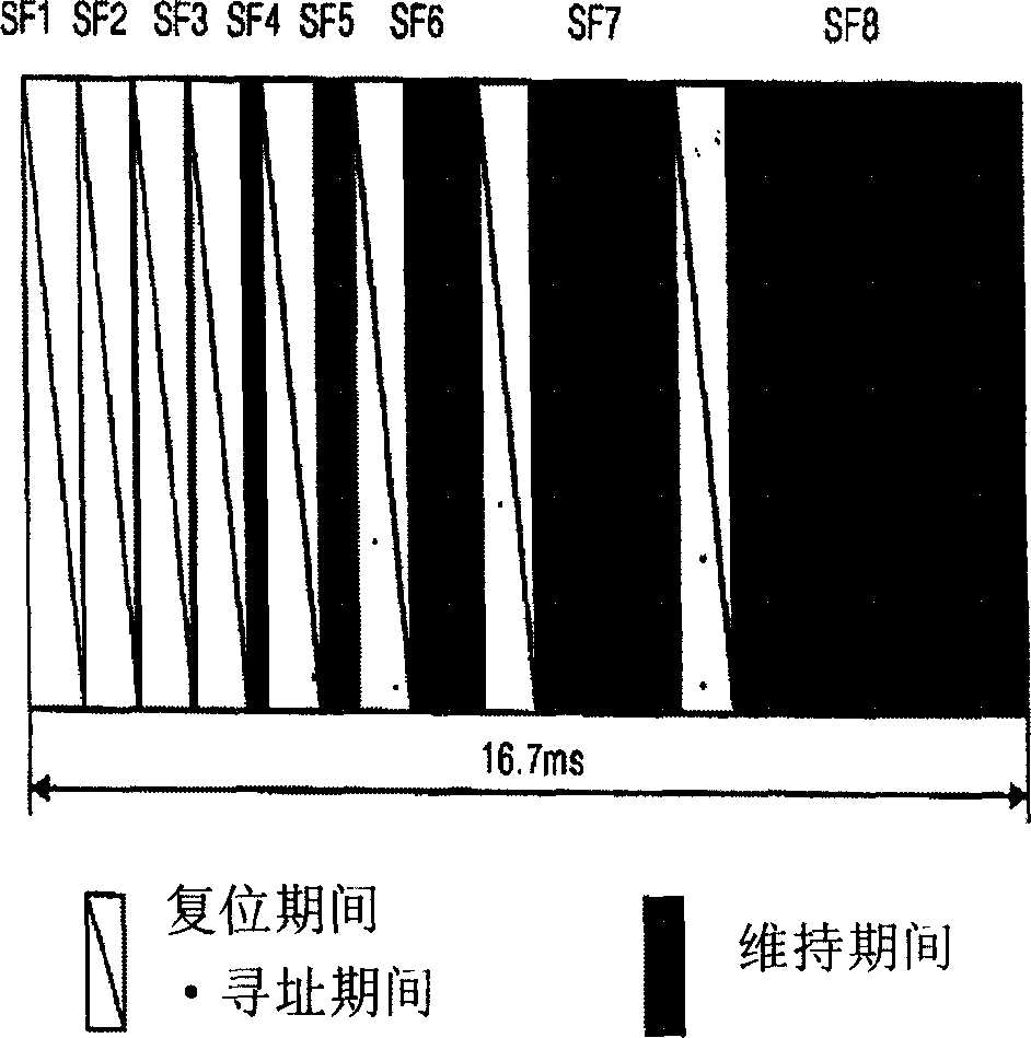
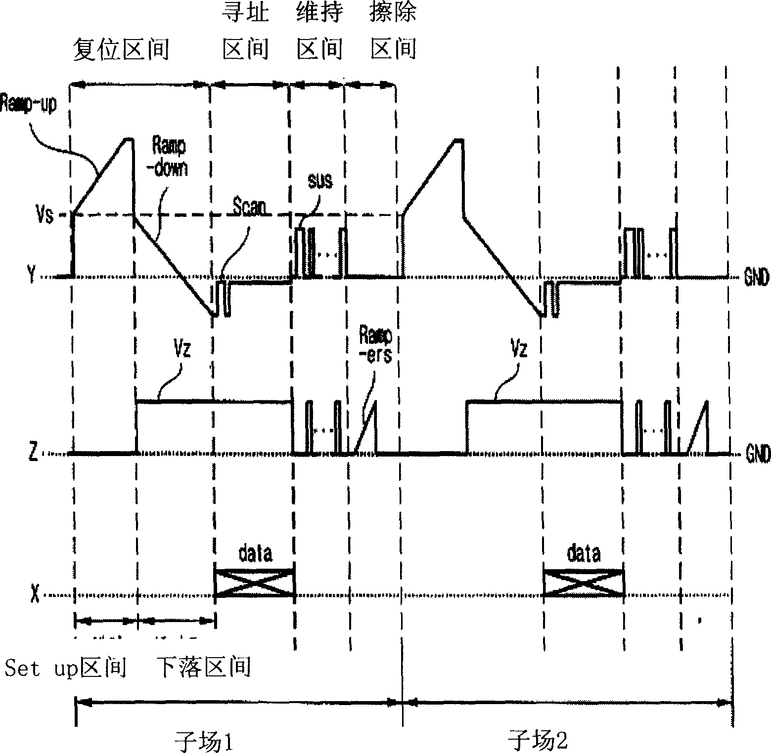
[0044] refer to Figure 6 to Figure 8 , the driving method of the plasma display panel is described in the first example of the invention. Figure 6 It is an explanatory diagram of driving waveforms within one frame in the driving method of the plasma display panel of the present invention. Figure 7 yes Figure 6 Partial enlarged view of part A in middle.
[0045] Figure 8 It is a diagram of the driving method of the plasma display panel of the present invention, and reset pulses are sequentially applied within a predetermined time period.
[0046] Such as Figure 6 As shown, when afterimages occur in the first frame and the second frame consecutive to the first frame, the second frame can apply a reset pulse at least in any subfield, and has the function of adjustment. For example, if 12 previous reset pulses are applied in 12 subfields with On cell in the first frame, after-image pattern will occur when the second frame in the next frame is Off cell. Here, the second...
PUM
 Abstract
Description
Claims
Application Information