Thin film transistor and its forming method

A technology of thin film transistors and semiconductors, applied in transistors, semiconductor/solid-state device manufacturing, optics, etc., to achieve the best resistance effect

Inactive Publication Date: 2006-11-08
CHUNGHWA PICTURE TUBES LTD
View PDF0 Cites 0 Cited by
  • Summary
  • Abstract
  • Description
  • Claims
  • Application Information

AI Technical Summary

Problems solved by technology

In addition, the above-mentioned problems al...

Method used


Image

  • Thin film transistor and its forming method
  • Thin film transistor and its forming method
  • Thin film transistor and its forming method

Examples


Embodiment Construction

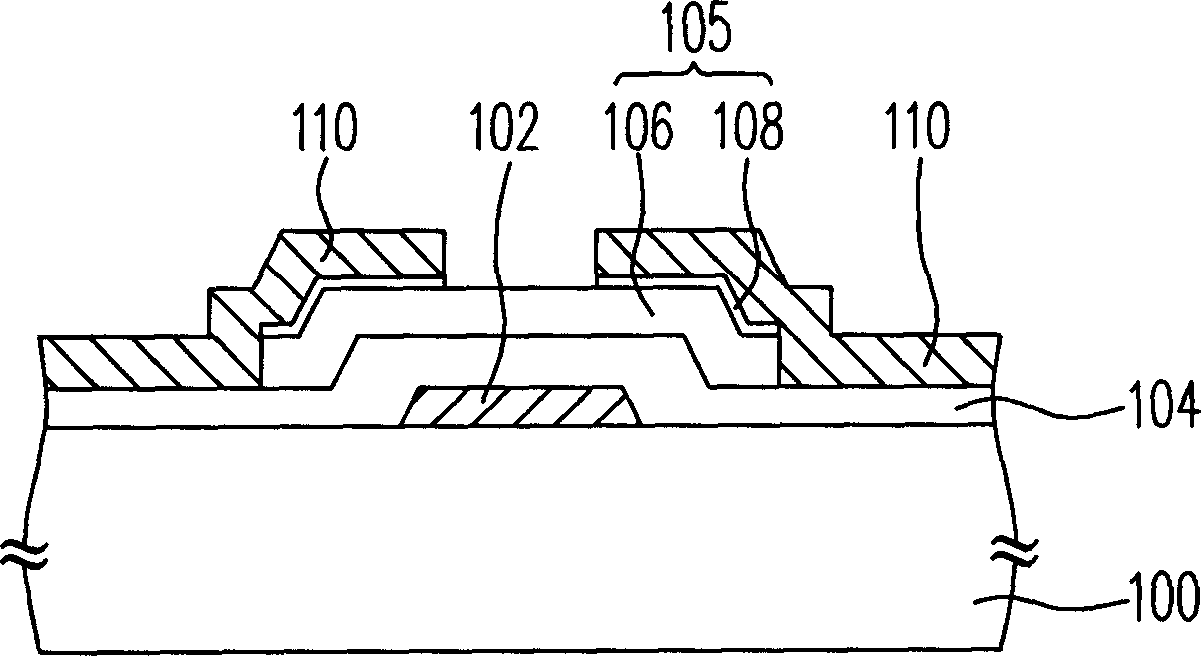
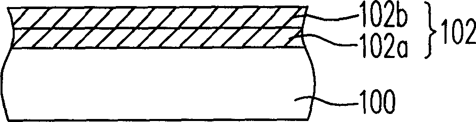
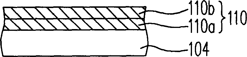
[0034] figure 1 It is a schematic cross-sectional view of a thin film transistor according to a preferred embodiment of the present invention. Please refer to figure 1 , the thin film transistor includes a gate 102 , a gate insulating layer 104 , a semiconductor layer 105 and a source / drain 110 . The gate 102 is disposed on the substrate 100 , and the gate insulating layer 104 is disposed on the substrate 100 to cover the gate 102 . The gate insulating layer 104 is made of, for example, a silicon oxide layer, a silicon nitride layer, or a combination layer of a silicon oxide layer and a silicon nitride layer. The semiconductor layer 105 is disposed on the gate insulating layer 104 above the gate 102 . The source / drain 110 is disposed on the semiconductor layer 105 . In this embodiment, the semiconductor layer 105 includes, for example, a channel layer 106 formed on the gate insulating layer 104 and an ohmic contact layer 108 formed between the channel layer 106 and the sou...


PUM


Abstract

A film transistor includes a grating, a grating insulation layer, a semiconduction layer and a source/drain, in which, the grating is set on the base and includes at least a layer of AlYN alloy, the grating insulation layer is formed on the base covering the grating, the semiconduction layer is set on the grating insulation layer on the base, the source/drain is set on the semiconductor, which has a grating and source/drain of a low contact resistor or line resistor.

Description

technical field [0001] The present invention relates to a semiconductor element and its manufacturing method, and in particular to a thin film transistor and its manufacturing method. Background technique [0002] A thin film transistor (TFT) generally includes a gate, a gate insulating layer, a channel layer, and a source / drain, and is usually used as a switching element in a display, such as a liquid crystal display (LCD). Generally, the method for forming a thin film transistor is to sequentially form a gate, a gate insulating layer, an α-Si channel layer, and a source / drain on a substrate. The gate is composed of a single metal layer of aluminum, chromium, tungsten, tantalum, titanium, etc. or a multi-layer metal layer. [0003] However, when a single layer of the above metal is used to form the gate, the surface of the film layer is easily corroded and reacts with oxygen to form a metal oxide, thus resulting in ineffective etching in the subsequent etching process. On...

Claims


Application Information

Patent Timeline
IPC IPC(8): H01L29/786G02F1/1368H01L21/336
Inventor 曹文光许泓译钟享显陈敏煌
Owner CHUNGHWA PICTURE TUBES LTD
Why Eureka
Try Eureka