Large-diameter zone-melting silicon single crystal growth method

A production method and a technology for a zone melting single crystal furnace, which are applied in the field of large-diameter zone melting silicon single crystal production, and can solve problems such as failure to achieve successful implementation.

Active Publication Date: 2006-11-22
ZHONGHUAN ADVANCED SEMICON MATERIALS CO LTD +1
View PDF1 Cites 29 Cited by
  • Summary
  • Abstract
  • Description
  • Claims
  • Application Information

AI Technical Summary

Problems solved by technology

As we all know, using the traditional preparation method of small-diameter zone-melting silicon single crystals below 3″, it is impossi

Method used


Image

  • Large-diameter zone-melting silicon single crystal growth method

Examples


Embodiment Construction

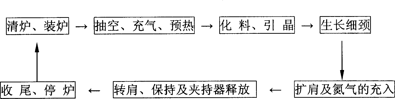
[0015] Refer to figure 1 .The process flow of melting silicon single crystal in large diameter zone is:

[0016] Furnace cleaning, furnace loading→evacuation, charging, preheating→materialization, seeding→growing necks→shoulder expansion and nitrogen filling→shoulder rotation, holding and release of holders→finishing and stopping the furnace.

[0017] (1) Furnace cleaning and furnace loading

[0018] Clean the entire furnace inner wall, heating coil, reflector, crystal holder, upper shaft, and lower shaft, adjust the level of heating coil and reflector, and align with the upper shaft and lower shaft.

[0019] Installation of polycrystalline materials:

[0020] ① Use scissors to cut open the plastic bag that packs the polycrystalline rods to expose only the grooves at the tail. Wear clean disposable plastic gloves, and fix the polycrystalline material clamp (crystal hanger) to the grooves at the tail of the polycrystalline rod. Place.

[0021] ②Insert the polycrystalline material c...


PUM


Abstract

The invention discloses a manufacturing method of silicon monocrystal, which comprises the following steps: 1. clearing furnace; loading furnace; 2. extracting; aerating; preheating; 3. digesting material; introducing seed; 4. growing thin neck; 5. expanding shoulder; aerating nitrogen; 6. transmitting; keeping; releasing clamper; 7. ending; stopping furnace. The invention realizes the large diameter zone melting silicon monocrystal, which reaches SEMI standard.

Description

Technical field [0001] The invention relates to a method for producing silicon single crystals, in particular to a method for producing large-diameter area molten silicon single crystals for the production of high-power, high-voltage, high-current semiconductor devices and various power electronic devices. technical background [0002] As one of semiconductor silicon materials, zone-melted silicon single crystal is mainly used as the main functional material of semiconductor power devices, power integrated devices and semiconductor integrated circuits. With the rapid development of the microelectronics industry, the semiconductor industry has also put forward newer and higher requirements for silicon materials. With the expansion of production scale, semiconductor device manufacturers are gradually requesting to increase the diameter of silicon wafers for the purpose of improving productivity, reducing costs, and increasing profits. For many years, the large-diameter crystal has ...

Claims


Application Information

Patent Timeline
IPC IPC(8): C30B13/00C30B29/06
Inventor 沈浩平高树良刘为钢高福林李翔汪雨田昝兴立
Owner ZHONGHUAN ADVANCED SEMICON MATERIALS CO LTD
Why Eureka
Try Eureka