Copper strike plating method
A technology of striking electroplating and copper layer, applied in circuits, electrical components, electric solid devices, etc., can solve the problems of increasing the lead frame manufacturing cost, consuming a lot of time, complicated lead frame steps, etc., and achieving the effect of improving the processing performance.
- Summary
- Abstract
- Description
- Claims
- Application Information
AI Technical Summary
Problems solved by technology
Method used
Image
Examples
example 1
[0065] A lead frame serving as a base material was obtained by subjecting a bar-shaped member made of a copper-nickel-silicon alloy (Corson alloy) containing 0.15% by weight of magnesium to press working. Next, heat treatment is performed in order to eliminate processing deformation of the lead frame. Next, only the lead frame is subjected to alkaline degreasing treatment and electrolytic activation treatment.
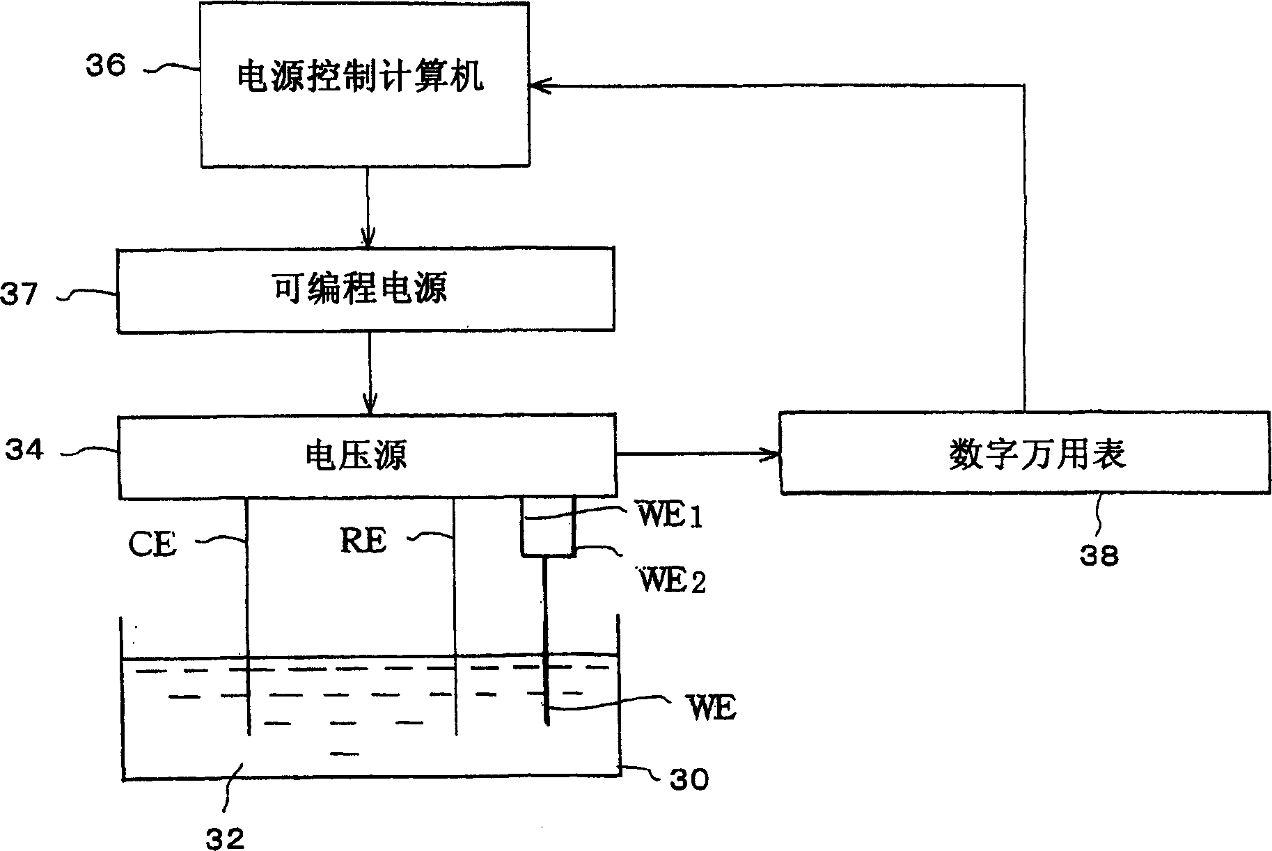
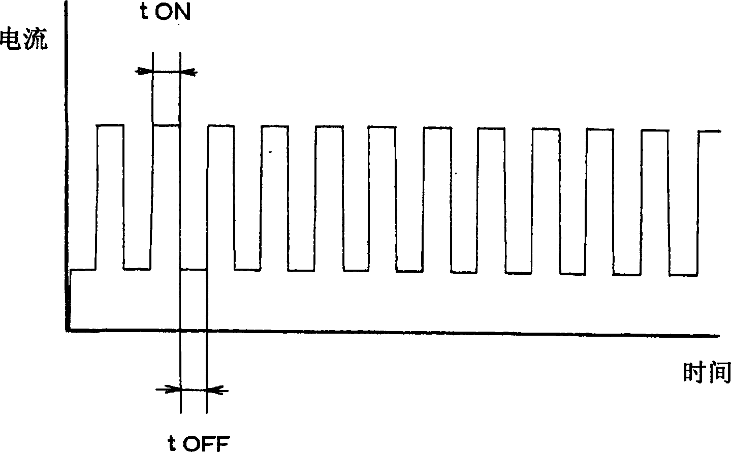
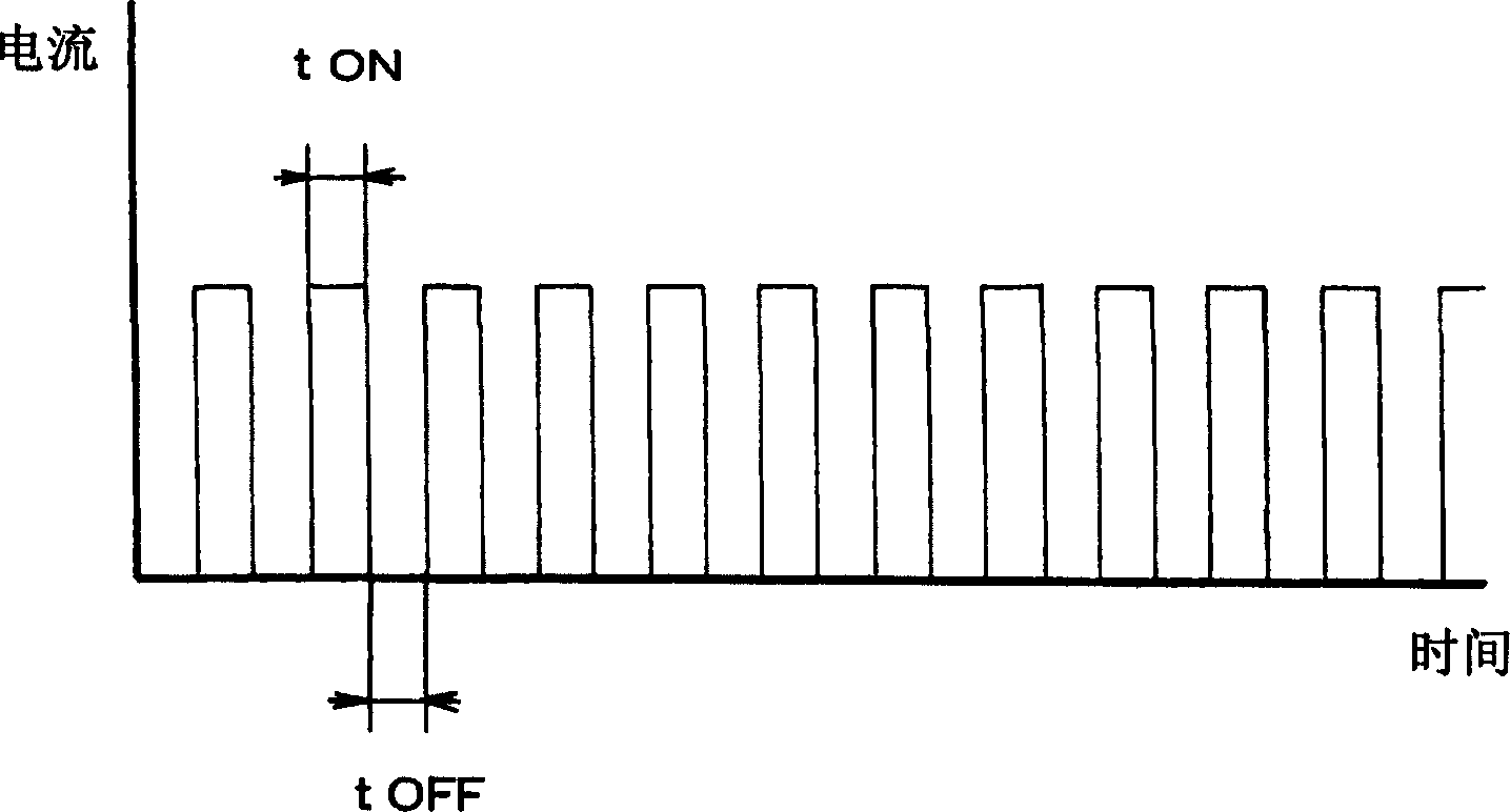
[0066] Next, when using figure 1 In the electrolytic copper plating equipment shown, the lead frame as the base material WE is inserted into the electroplating tank 30 in which the electrolytic copper plating solution is stored, and then copper strike plating is performed on the surface of the lead frame by applying a pulse current.
[0067] At this time, in the copper strike plating, the pulse period of the pulse current was set to 100 Hz, and the average current density (C.D.) was set to 7 A / dm 2 . Next, when the duty ratio was changed from 0.2 to 1.0, a 0.5 μm th...
example 2
[0074] In Example 2, copper strike plating and electrolytic silver plating were performed in a similar manner to Example 1, except that the pulse period was changed as shown in Table 2 while maintaining a duty ratio of 0.4. Table 2 also shows the results of visual observation regarding the appearance of the copper strike plating layer and the appearance of the silver plating layer, as well as distribution ranges of nodules (surface roughness), height differences, and gloss unevenness showing abnormal deposition of silver. In Table 2, ○ indicates good, △ indicates slightly recognizable abnormal deposits, and X indicates recognizable abnormal deposits.
[0075] Preface
[0076] It is evident from Table 2 that good copper strike plating can still be formed when the pulse period varies from 1 to 1000 Hz even without polishing the heat-treated leadframe. In this way, a good silver plating layer can be formed on the copper strike plating layer.
example 3
[0081] In Example 3, the pulse period of the pulse current supplied to the lead frame was set to 100Hz, and the average current density (C.D.) was set to 7A / dm 2 , and under the condition that the duty ratio is set to 0.4, a 0.1 μm thick copper strike plating layer is formed by implementing copper strike plating, and a 3 to 5 μm thick electroplating layer is formed on the copper strike plating layer by electrolytic silver plating For the silver layer, plating was performed on the lead frame by setting other conditions similar to Example 1 except the above.
[0082] Next, a copper oxide film was formed on the plated lead frame under the heating conditions given in Table 3, followed by peeling off the tape adhering to the lead frame to perform a tape peel test to detect whether the plated layer was peeled off . Thus, the adhesion of the copper strike plating layer to the oxide film was evaluated. The evaluation results are also given in Table 3.
[0083] heating stri...
PUM
| Property | Measurement | Unit |
|---|---|---|
| thickness | aaaaa | aaaaa |
| thickness | aaaaa | aaaaa |
| thickness | aaaaa | aaaaa |
Abstract
Description
Claims
Application Information
 - R&D Engineer
- R&D Manager
- IP Professional
- Industry Leading Data Capabilities
- Powerful AI technology
- Patent DNA Extraction
Browse by: Latest US Patents, China's latest patents, Technical Efficacy Thesaurus, Application Domain, Technology Topic, Popular Technical Reports.
© 2024 PatSnap. All rights reserved.Legal|Privacy policy|Modern Slavery Act Transparency Statement|Sitemap|About US| Contact US: help@patsnap.com


