Opto-electronic device comprising a laser integrated with a modulator and method of fabrication thereof

一种集成调制器、光电设备的技术,应用在激光器、激光器零部件、半导体激光器等方向,能够解决难以完全控制外延生长、寄生电容不允许高吞吐量使用、复杂制作工艺等问题

Inactive Publication Date: 2007-01-10
ALCATEL LUCENT SAS
View PDF2 Cites 12 Cited by
  • Summary
  • Abstract
  • Description
  • Claims
  • Application Information

AI Technical Summary

Problems solved by technology

However, these structures with excellent properties require complex fabrication processes, including epitaxial growth that is difficult to fully control and additional steps to trim the vertical confinement layer.
This technique also yields structures whose excessive parasitic capacitance does not allow high-throughput use of

Method used


Image

  • Opto-electronic device comprising a laser integrated with a modulator and method of fabrication thereof
  • Opto-electronic device comprising a laser integrated with a modulator and method of fabrication thereof
  • Opto-electronic device comprising a laser integrated with a modulator and method of fabrication thereof

Examples


Embodiment Construction

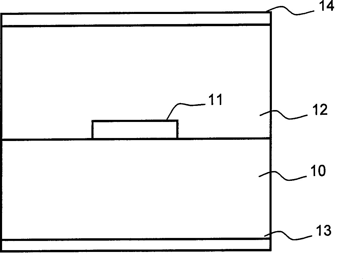
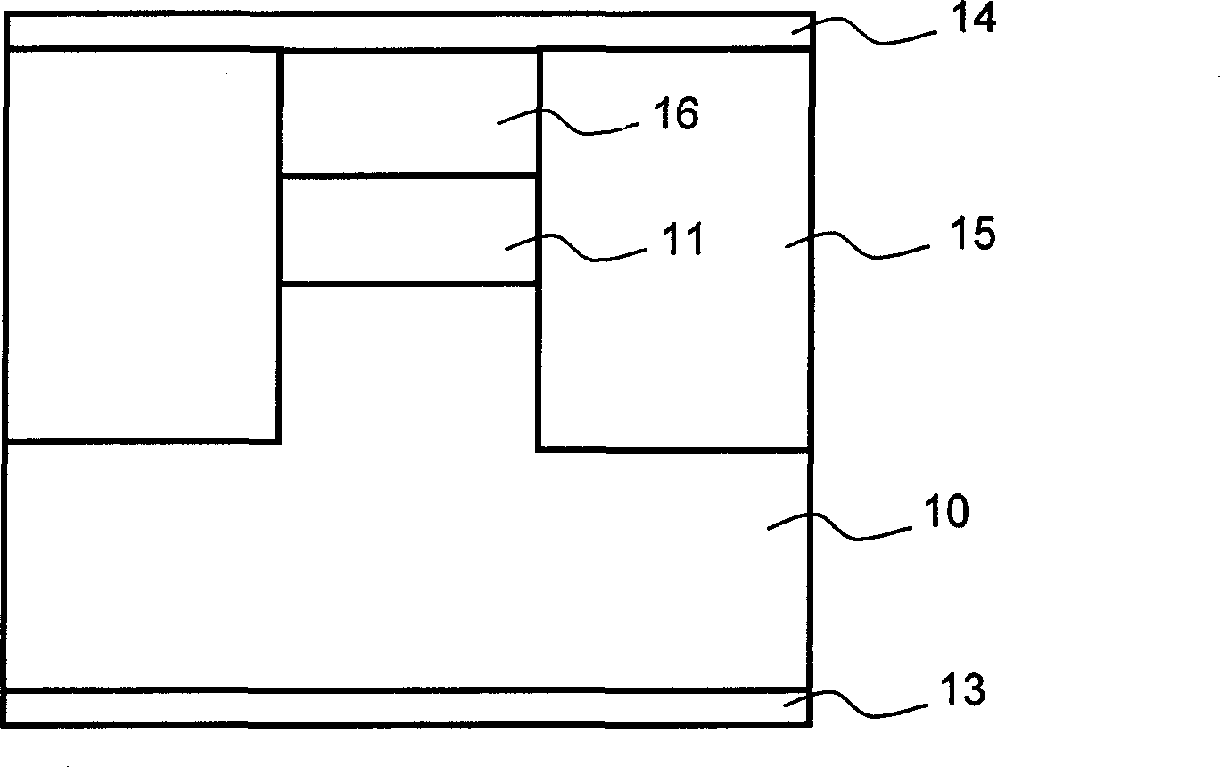
[0050] Figure 4 The sectional view of shows an ILM type device according to the invention, comprising a laser part and a modulating part. It mainly consists of generic structures of the P.I.N type, which in succession include:

[0051] a substrate 10 made of n-doped semiconductor material,

[0052] a buried active region 11 formed by strips of rectangular cross-section,

[0053] • A p-doped vertical confinement layer 16, the sides of the active region surrounded by a semi-insulating lateral confinement layer (not shown in the figure) made of doped semiconductor material.

[0054] The laser part comprises a barrier layer 17 made of n-doped semiconductor material interposed between a semi-insulating lateral confinement layer and a vertical confinement layer.

[0055] The substrate, vertical confinement layer, lateral confinement layer and barrier layer are mainly made of a first semiconductor material whose composition belongs to groups III and V of the periodic table. For ...


PUM


Abstract

The field of the invention is that of integrated optical emission devices comprising a laser emission section and a section for modulating the optical power emitted by the laser, also known as ILM devices, the acronym standing for Integrated Laser Modulator. The invention is aimed at an ILM device comprising a laser section (1) and a modulation section (2) such as electro absorption modulator, formed in a PIN type common structure, where the structure successively comprises a substrate (10) in n doped semiconductor material, buried active zone (11) and p doped vertical confinement layer (16) and a semi-insulating lateral confinement layer (15). The laser section has a blocking layer (17) in n doped semiconductor material disposed between the semi-insulating lateral confinement layer and vertical confinement layers. The performance and the reliability of the final device is thus improved.

Description

technical field [0001] The field of the invention is a light emitting device comprising an integrated component comprising at least one laser emitting part and a part for modulating the optical power emitted by the laser. These systems are also known as ILM (short for Integrated Laser Modulator) or EML (short for Electro-absorption Modulated Laser). The modulating section is often referred to as EAM (short for ElectroAbsorption Modulator). [0002] These devices are primarily used in high-throughput digital communications. Throughput typically ranges from a few gigabits to tens of gigabits per second. Background technique [0003] The laser beam can be modulated in three different ways. The first method involves direct modulation of the source laser by controlling the feed current of the source laser. However, this technique does not allow it to achieve the performance necessary for high throughput. It is also possible to use an external modulator physically separate fr...

Claims


Application Information

Patent Timeline
Patent Type & Authority Applications(China)
IPC IPC(8): H01S5/32H01S5/026H01S5/323H01S5/00H04B10/02
CPCH01S5/2222H01S5/3072H01S5/227H01S5/0265H01S5/2224
Inventor 米夏埃尔·勒帕莱克克里斯托夫·卡兹米耶斯基
Owner ALCATEL LUCENT SAS
Why Eureka
Try Eureka