Over boosting prevention circuit

A booster circuit and circuit technology, applied in logic circuits, electrical components, conversion equipment without intermediate conversion to AC, etc., can solve problems such as inability to share reference voltages, and achieve the effect of preventing misoperation

Inactive Publication Date: 2007-01-10
SANYO ELECTRIC CO LTD
View PDF2 Cites 0 Cited by
  • Summary
  • Abstract
  • Description
  • Claims
  • Application Information

AI Technical Summary

Problems solved by technology

[0013] In addition, in addition to the above-mentioned reference voltage (Vref+Vout) used in this overvoltage prevention circuit, when the reference voltage Vref based on Vss is required, since the reference voltage cannot be shared, there is also a possibility that the reference voltage must be made in another way. The problem with the reference voltage Vref

Method used


Image

  • Over boosting prevention circuit
  • Over boosting prevention circuit
  • Over boosting prevention circuit

Examples


Embodiment Construction

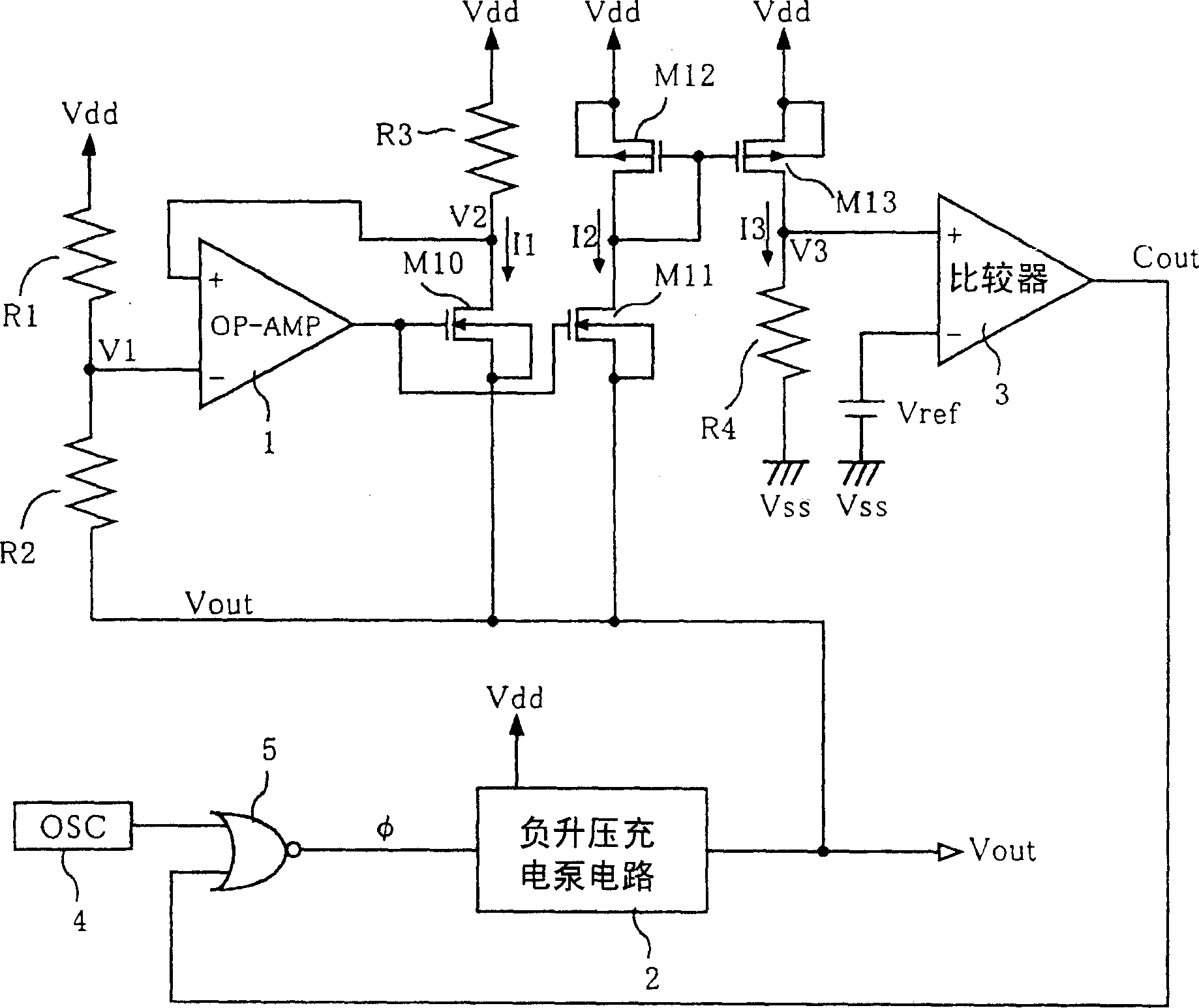
[0033] Before describing the embodiment of the present invention, an overvoltage prevention circuit related to a reference example will be described. Figure 10 is the circuit diagram of this overvoltage prevention circuit. Resistors R1 and R2 are connected in series between the output voltage Vout (<0V) and Vdd of the charge pump circuit 60 for negative boosting, and a voltage V0' is generated at the connection point, and the voltage V0' and the following voltage are generated by the comparator 61. Vout is compared with a reference voltage (Vref+Vout) as a reference, and the output of the comparator 61 controls the supply of the boost clock φ to the charge pump circuit 60 .

[0034]That is, when V0'>Vref+Vout, the output of the comparator 61 is H (high), and the boost clock φ is supplied to the charge pump circuit 60, so the charge pump circuit 60 performs a boost operation.

[0035] According to the boosting operation of the charge pump circuit 60, when V0'


PUM


Abstract

An overboosting prevention circuit is provided in the invention to control the difference (Vdd-Vout) between the power supply voltage Vdd and the output voltage Vout (<0V) of the charge pump circuit 2 does not exceed a predetermined value VMAX. That is, the charge pump circuit 2 performs boosting operation when Vdd-VoutVMAX. An influence of the ripples caused in the charge pump circuit 2 is removed because the reference voltage Vref to an operational amplifier is determined relative to a ground voltage Vss. Therefore, the invention can prevent malfunction in an overboosting prevention circuit by removing ripples occurring in the boosting circuit.

Description

technical field [0001] The present invention relates to an over-boost preventing circuit for preventing over-boosting of a boosting circuit that generates a negative output voltage relative to a ground voltage according to a boosting clock. Background technique [0002] Conventionally, a charge pump (charge pump) circuit is known as a type of booster circuit that boosts the power supply voltage several times. Charge pump circuits are widely used, for example, as power supply circuits of portable electronic devices. In a general charge pump circuit, a plurality of switching elements are connected in series, a boost clock is supplied to each connection node of these switching elements through a capacitor, and charge is transferred through the switching elements to boost an input power supply voltage. [0003] However, a high voltage as a result of boosting is applied to a transistor used as a switching element of the charge pump circuit or a transistor constituting a circuit ...

Claims


Application Information

Patent Timeline
Patent Type & Authority Applications(China)
IPC IPC(8): H03K19/094
CPCH02M3/07H03K19/094
Inventor 河井周平
Owner SANYO ELECTRIC CO LTD
Why Eureka
Try Eureka