Electron emission device

A technology of electron emission device and electrode, which is applied in the direction of photoelectric emission cathode, tube without control device, circuit, etc., to achieve the effect of high output

Inactive Publication Date: 2007-02-07
KK TOSHIBA
View PDF2 Cites 2 Cited by
  • Summary
  • Abstract
  • Description
  • Claims
  • Application Information

AI Technical Summary

Problems solved by technology

[0011] In addition, in the invention described in Patent Document 2, in order to emit secondary electrons, it is necessary to collide with primary electrons, but there is a problem in this case that it is difficult to make primary electrons having energy for emitting secondary electrons, Hit the diamond partition equally and evenly

Method used


Image

  • Electron emission device
  • Electron emission device
  • Electron emission device

Examples


no. 1 Embodiment approach

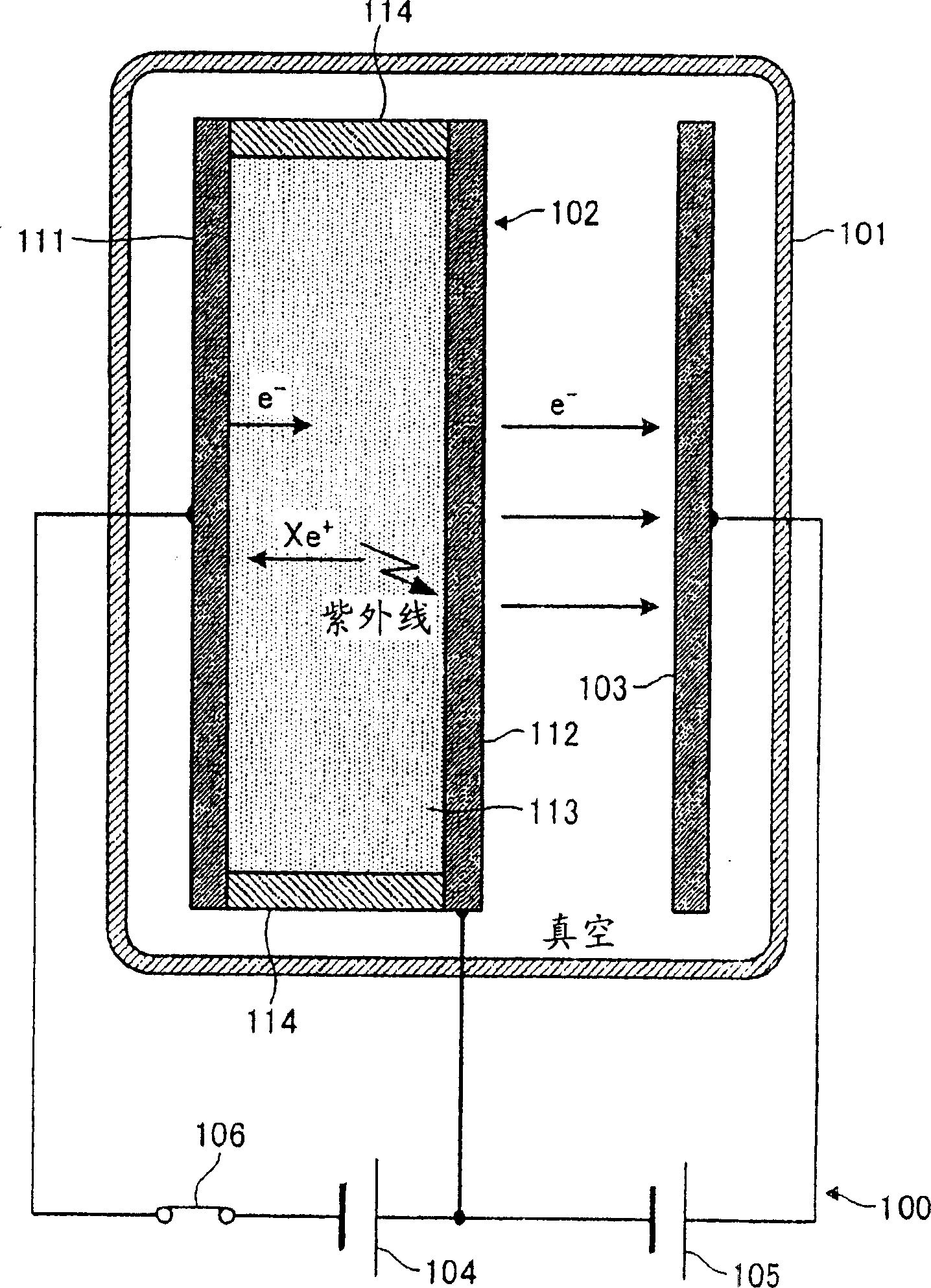
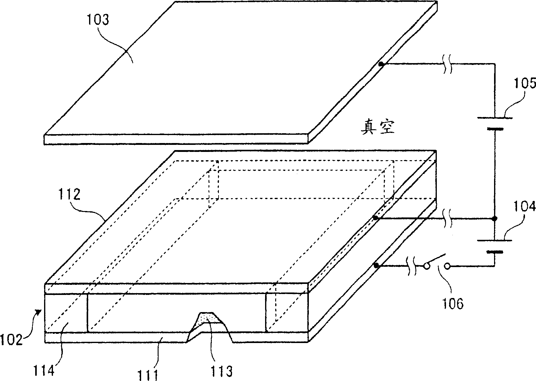
[0028] figure 1 It is a side cross-sectional view of the electron emission device 100 of the first embodiment. As shown in this figure, the electron emission device 100 has a discharge unit (cell) 102 and a discharge anode 103 inside a vacuum airtight container 101, and has an off switch 106 and a first power supply 104 outside the airtight container 101. and the second power supply 105 . In addition, since this figure is prepared for ease of explanation, the dimensional ratios in the figure are not necessarily consistent with the description or other Figure 1 Sincerely.

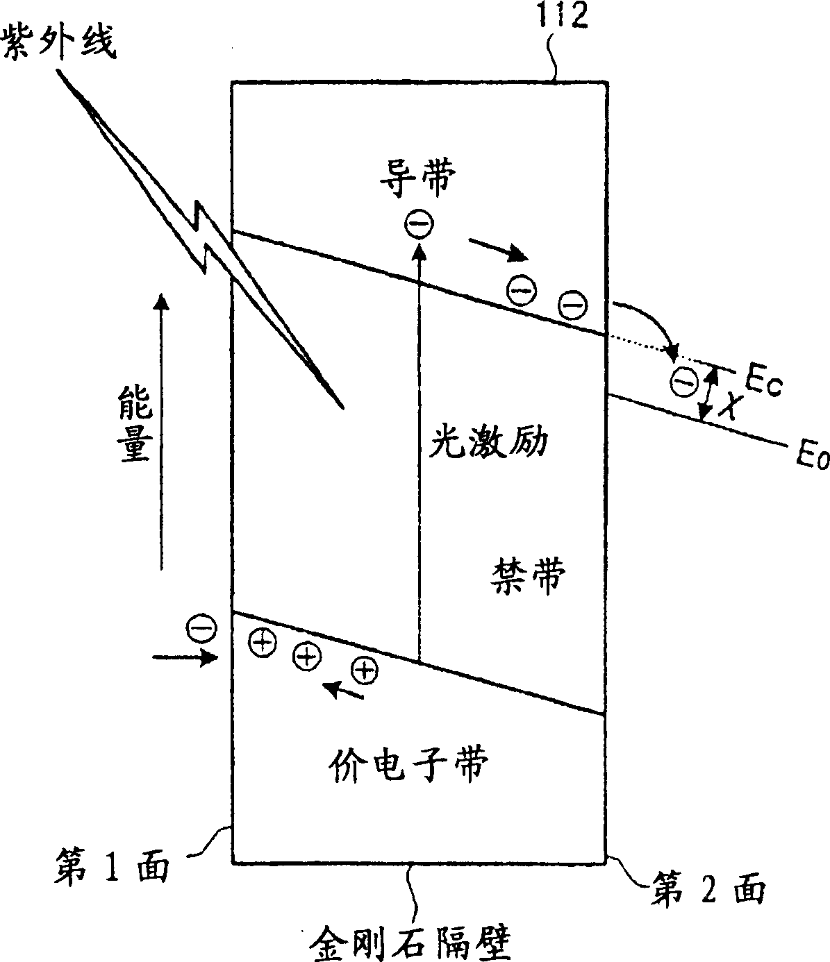
[0029] The airtight container 101 forms a vacuum inside the container for emitting electrons in the vacuum. The shape, size, and material of the airtight container 101 are not limited as long as the container can be vacuumed. For example, in the case where a phosphor is coated on the discharge anode 103, it is also possible to make the emitted electrons collide with the phosphor so that the user can see...

no. 2 Embodiment approach

[0060] In addition, the electron emission device 100 according to the first embodiment generally does not control when emitting electrons after the power supply circuit is turned on by the switch 106 for shutting off. However, the present invention is not limited to such a configuration, and may have a configuration for efficiently starting electron emission, and use this configuration to perform control at the time of electron emission. Therefore, in the second embodiment, a case where a trigger switch is provided and the current on the control circuit is switched by the trigger switch will be described.

[0061] Figure 5 It is a side cross-sectional view of the electron emission device 500 of the second embodiment. The difference from the electron emission device 100 of the first embodiment described above is that it has a configuration in which a trigger switch 501 is added. In the following description, the same reference numerals are assigned to the same constituent el...

no. 3 Embodiment approach

[0067] In the electron emission device of the above-described embodiment, the amount of emitted electrons can be adjusted only by using the off switch 106 to perform on / off control of electron emission. However, the present invention is not limited to such control, and a mechanism for controlling the amount of current, that is, the amount of electron emission may be provided. Therefore, in the third embodiment, a case where the emission amount of electrons is controlled by providing a variable resistor will be described.

[0068] Figure 7 It is a side cross-sectional view of the electron emission device 700 of the second embodiment. The difference from the electron emission device 500 of the second embodiment described above is that it has a structure in which a variable resistor 701 is added and an off switch 702 is arranged differently from the off switch 106 . In the following description, the same reference numerals are assigned to the same constituent elements as those...


PUM


Abstract

The invention is to achieve stable emission of electrons and a high output of electrons even with impression at low voltage. The electron emission device includes a first electrode; a semiconductor barrier that has a first face disposed to face the first electrode and a second face which is opposite face of the first face, and is formed with a wide bandgap semiconductor; an insulating material that forms a space sealed between the first electrode and the semiconductor barrier; an inert gas that is encapsulated in the space; a second electrode that is disposed to face a second face of the semiconductor barrier interposing vacuum therebetween; a first voltage applying unit that applies a voltage between the first electrode and the semiconductor barrier; and a second voltage applying unit that applies a voltage between the semiconductor barrier and the second electrode.

Description

technical field [0001] The present invention relates to an electron-emitting device that emits electrons in a vacuum, and more particularly, to a technology for emitting electrons from a planar type (emitting surface) by applying a voltage. Background technique [0002] Conventionally, a vacuum electron source that emits electrons in a vacuum has been used as a component of various devices. Furthermore, since the vacuum electron emission source is a main technical point in various devices, various technological developments have been continuously carried out in order to improve the performance of the devices. [0003] The principle itself of this electron emission can be roughly classified into thermionic emission or electric field electron emission, or electric field thermionic emission in between. First, thermionic emission is by heating the cathode to impart energy beyond the work function to the cathode, resulting in the emission of electrons. Therefore, it is not nece...

Claims


Application Information

Patent Timeline
Patent Type & Authority Applications(China)
IPC IPC(8): H01J1/00H01J1/30H01J1/34
CPCH01J21/04H01J3/021
Inventor 酒井忠司小野富男佐久间尚志吉田博昭铃木真理子
Owner KK TOSHIBA
Why Eureka
Try Eureka