Thin film field emitting cathode with gradually changed electronic transmission layer component

A technology of electron transport layer and field emission cathode, which is applied in the direction of discharge tube/lamp parts, cathode ray tube/electron beam tube, circuit, etc., can solve the problem that the emission current of large-screen high-brightness flat-panel display devices cannot be satisfied, Achieve the effect of low device capacitance and large emission current

Inactive Publication Date: 2002-06-05
TSINGHUA UNIV
View PDF1 Cites 5 Cited by
  • Summary
  • Abstract
  • Description
  • Claims
  • Application Information

AI Technical Summary

Problems solved by technology

The inventor has improved this structure (patent application number 00103365.4 publication number CN 1265521A), reached more than 50aμA / cm 2 emission current, but still cannot meet the emission current required by large-screen high-brightness flat-panel display devices, and its performance still needs further improvement

Method used


Image

  • Thin film field emitting cathode with gradually changed electronic transmission layer component
  • Thin film field emitting cathode with gradually changed electronic transmission layer component
  • Thin film field emitting cathode with gradually changed electronic transmission layer component

Examples


specific Embodiment approach

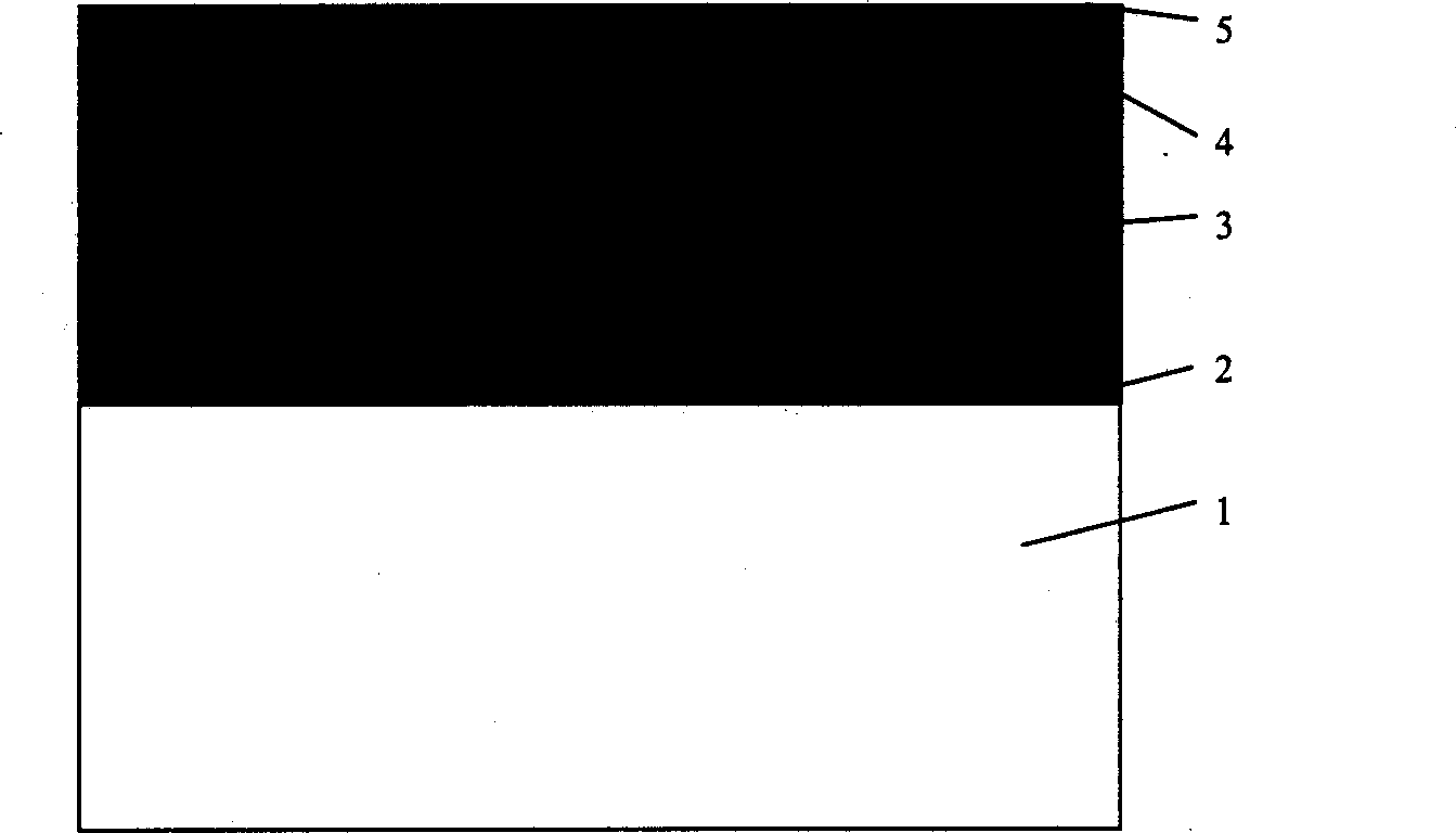
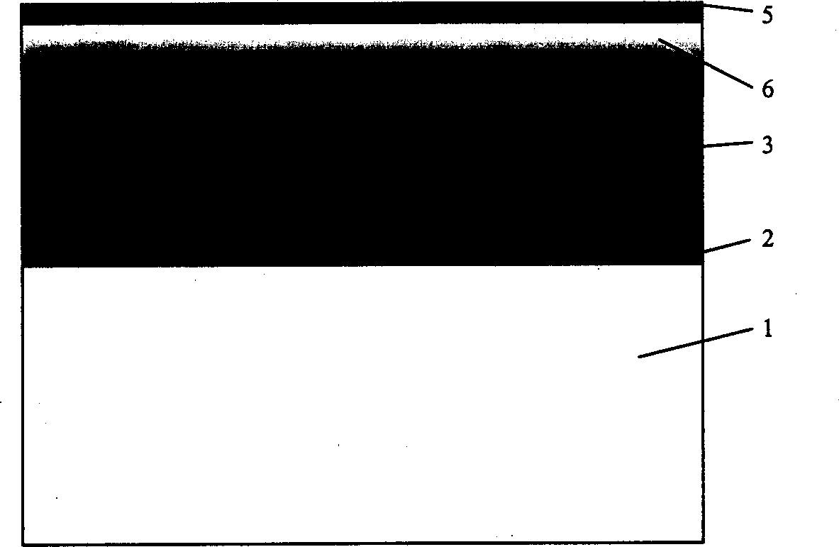
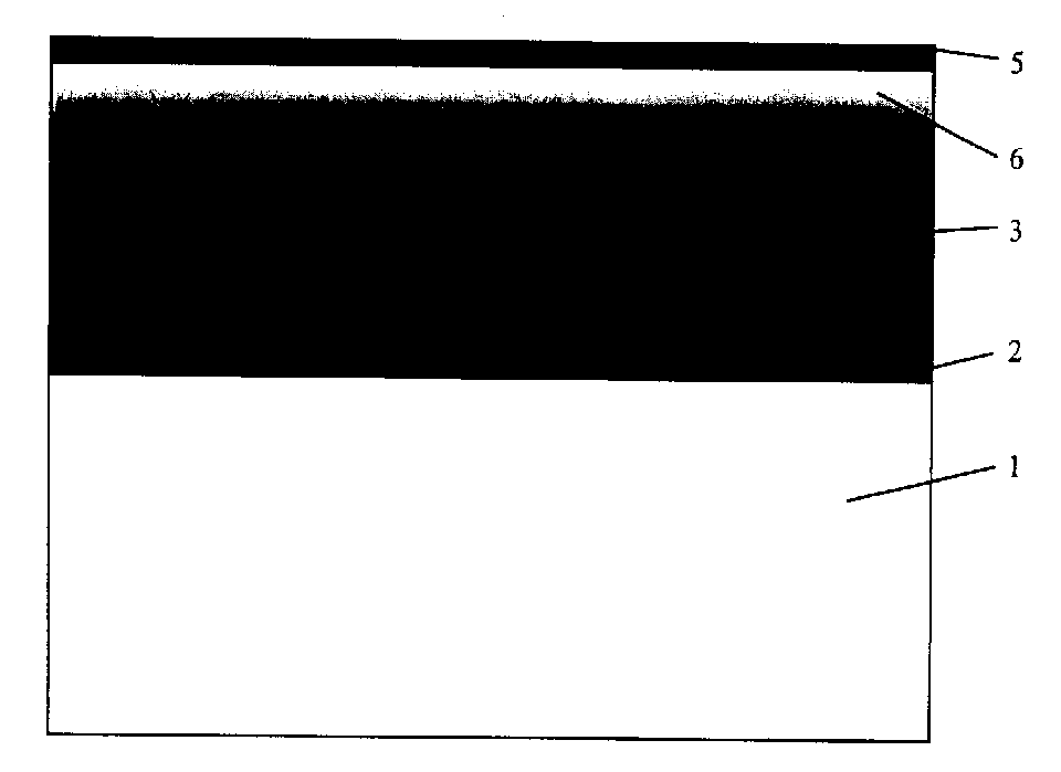
[0018] The electronic transport layer composition graded thin film field emission cathode of the present invention comprises a substrate glass 1 , a lower electrode 2 , a single component insulating layer 3 , a composition graded electron transport layer 6 and an upper electrode 5 .

[0019] In this structure, when a reverse voltage is applied between the upper and lower electrodes, electrons are injected from the upper electrode into the conduction band of the electron transport layer, and finally reach the interface between the electron transport layer and the single-component insulating layer. These electrons cannot enter the single-component insulating layer, but form electrons on the interface state energy level. When a forward voltage is applied between the electrodes, the electrons in the interface state return to the electron transport layer of the graded component and are accelerated there to obtain sufficient kinetic energy. Since the electron affinity of the materia...

Embodiment 1

[0021] The lower electrode uses a metal molybdenum film with a thickness of 100 nanometers, the single-component insulating layer 3 is a tantalum pentoxide film with a thickness of 400 nanometers, and the composition-graded electron transport layer 6 adopts 100 nanometers of semiconductor zinc sulfide with high electron affinity to low electron affinity. Potential for semiconducting magnesium sulfide graded transition films. The upper electrode 5 adopts a semiconductor hafnium nitride film with a thickness of 10 nanometers and a low work function. If the ratio of the emission current to the current between the electrodes is defined as the emissivity, at a driving voltage of 80 volts, a field emission current with an emissivity greater than 0.5% is obtained.

Embodiment 2

[0023] The lower electrode uses a metal chromium film with a thickness of 100 nanometers, the single-component insulating layer 3 is a tantalum pentoxide film with a thickness of 400 nanometers, and the composition-gradient electron transport layer 5 adopts a film with a gradual transition from zinc sulfide to magnesium sulfide with a thickness of 50 nanometers. The upper electrode 5 adopts a metal silver film with a thickness of 10 nanometers. Under a driving voltage of 120 volts, a field emission current with an emissivity greater than 0.5% is obtained.


PUM


Abstract

A film field emission cathode with ingredient gradually changed in electron transport layer belongs to the technique area of vacuum electron emission type of flat display device, especially in relates to the structural design of plane type field emission cathode. The invention is composed of base plate glass, lower metal electrode, insulated layer with single component, electron transport layer and upper electrode. The medium film the ingredient gradually changed is adopted in electron transport layer, i.e. from button to top of the medium film, the ingredient of high electric affinity is changed to that of lower electric affinity. Metal or semiconductor film with lower work function is adopted in the upper electrode. The invention possesses features of large emissive current, long service life and lower cost. It is suitable for producing field emission type flat display device with large area.

Description

technical field [0001] The invention belongs to the technical field of vacuum electron emission flat panel display, and in particular relates to a novel planar field emission cathode structure. Background technique [0002] Field emission cathodes have structures such as microtip type (Spindt type), diamond film type, carbon nanotube type, metal-insulator-metal type (MIM) and metal-insulator-semiconductor layer-metal type (MISM). Which is closer to the present invention is an AC-driven MISM structure, such as figure 1 shown. It includes a glass substrate 1 , a metal lower electrode 2 , an insulating layer 3 , a semiconductor layer (electron transport layer) 4 and a metal upper electrode 5 . [0003] In the existing AC-driven MISM structure, the metal lower electrode is generally made of aluminum, gold, molybdenum, etc., the upper electrode is made of gold, platinum, aluminum, etc., the insulating layer is made of tantalum pentoxide, and the semiconductor layer (electron tr...

Claims


Application Information

Patent Timeline
Patent Type & Authority Applications(China)
IPC IPC(8): H01J1/304H01J29/04
Inventor 李德杰
Owner TSINGHUA UNIV
Why Eureka
Try Eureka