

A field emission electron source emitter tip shaping device and its shaping method
An electron source and field emission technology, applied in the manufacture of circuits, electrical components, electrode systems, etc., can solve the problems of unstable work and large emission beam current, and achieve high angular current density, large emission current, and concentrated emission direction Effect
- Summary
- Abstract
- Description
- Claims
- Application Information
AI Technical Summary
Problems solved by technology
Method used
Image

Examples
Embodiment Construction
[0039] The present invention will be further described through the embodiments below in conjunction with the accompanying drawings.
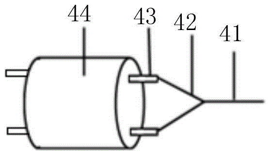
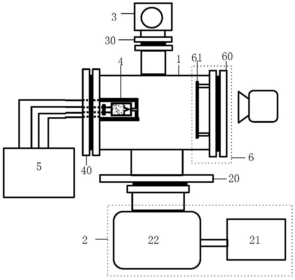
[0040] Such as figure 2 As shown, the field emission electron source emitter tip shaping device of this embodiment includes: a vacuum chamber 1, a vacuum pumping system 2, a vacuum degree measurement system 3, an electron gun assembly 4, a power supply system 5 and an electron beam imaging system 6; Wherein, the lower surface of the vacuum chamber 1 is connected to the vacuum pumping system 2 through the flange port 20, and the upper surface is connected to the vacuum degree measuring system 3 through the flange port 30; the electron gun assembly 4 is installed in the vacuum chamber 1 through the electron gun flange port 40 and connected to the power system 5 outside the vacuum chamber through conductive leads; on the surface of the vacuum chamber opposite to the electron gun assembly, an electron beam imaging system 6 is installed through the ...
PUM
 Abstract
Description
Claims
Application Information