Silicon carbide junction barrier Schottky diode suitable for high-temperature environment

A junction barrier Schottky and high-temperature environment technology, which is applied in the direction of electrical components, circuits, semiconductor devices, etc., can solve the problems of silicon carbide junction barrier diode performance degradation, etc., to increase the Schottky contact area and solve the problem of positive The effect of increasing the forward conduction power and increasing the area of ​​the depletion region towards the current decay

Active Publication Date: 2022-04-05
UNIV OF ELECTRONICS SCI & TECH OF CHINA
View PDF15 Cites 2 Cited by
  • Summary
  • Abstract
  • Description
  • Claims
  • Application Information

AI Technical Summary

Problems solved by technology

[0005] Therefore, how to solve the problem of the performance degradation of silicon carbide junction barrier diodes in high temperature environments has become an urgent technical problem to be solved.

Method used


Image

  • Silicon carbide junction barrier Schottky diode suitable for high-temperature environment
  • Silicon carbide junction barrier Schottky diode suitable for high-temperature environment
  • Silicon carbide junction barrier Schottky diode suitable for high-temperature environment

Examples


Embodiment Construction

[0032] Embodiments of the present invention are described below through specific examples, and those skilled in the art can easily understand other advantages and effects of the present invention from the content disclosed in this specification. The present invention can also be implemented or applied through other different specific implementation modes, and various modifications or changes can be made to the details in this specification based on different viewpoints and applications without departing from the spirit of the present invention.

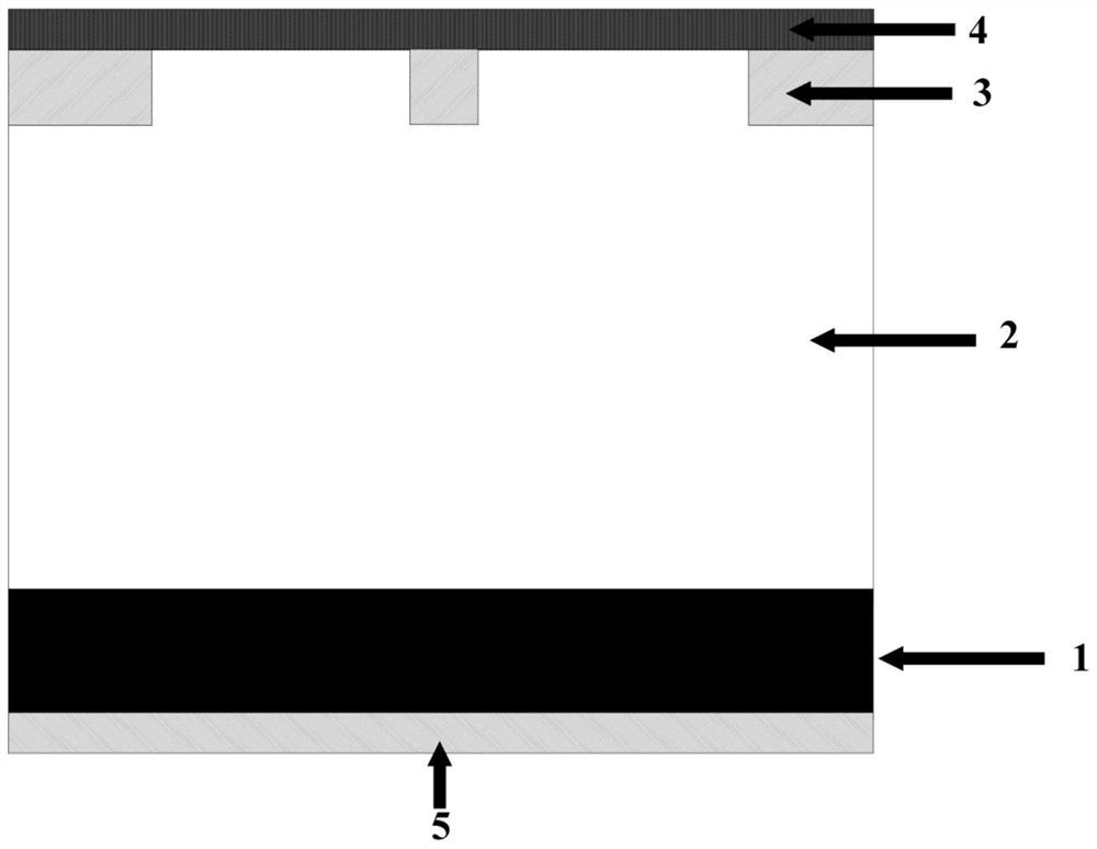
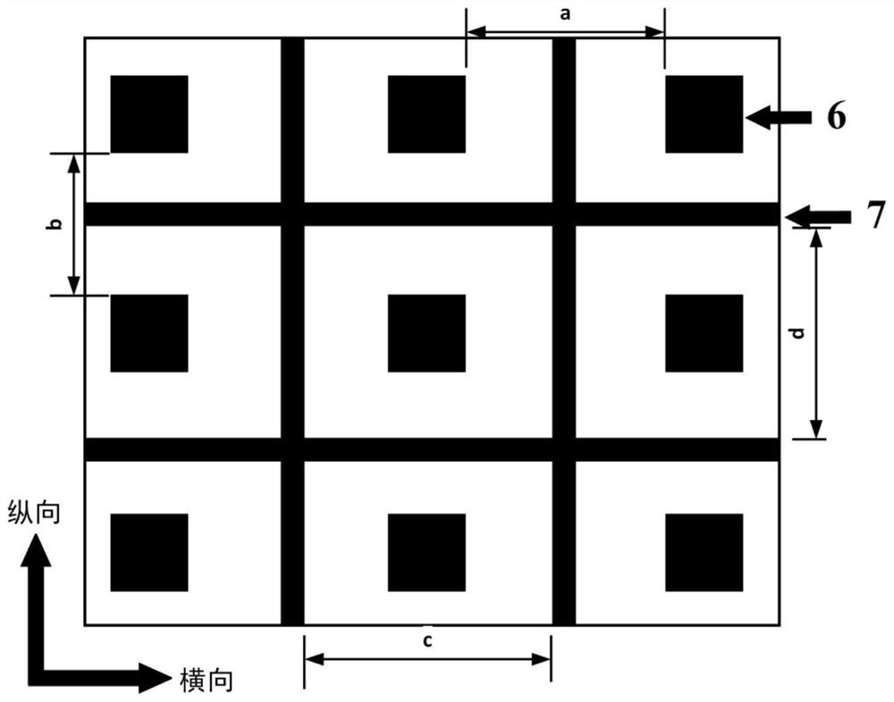
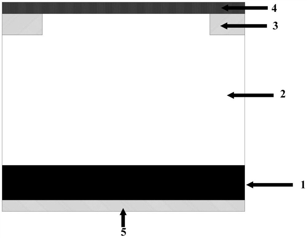
[0033] Such as figure 1 and image 3 As shown, the embodiment of the present invention provides a silicon carbide junction barrier Schottky diode suitable for high temperature environment, a silicon carbide junction barrier Schottky diode suitable for high temperature environment, including ohmic contact electrode 5, carbonization Silicon N+ substrate 1, silicon carbide N- epitaxial layer 2, Schottky contact electrode 4 and multiple ...


PUM

PropertyMeasurementUnit
thicknessaaaaaaaaaa

Abstract

The invention relates to a silicon carbide junction barrier Schottky diode suitable for a high-temperature environment, and belongs to the technical field of semiconductor devices. According to the device, a novel P + region injection layout structure is adopted on the basis of a traditional JBS device structure, the area of a Schottky contact region and Schottky junction current are increased, meanwhile, the area of a depletion region is increased through a strip-shaped pattern of the P + injection region, the current decline and power loss increase of a silicon carbide junction barrier Schottky diode at high temperature are reduced, and the performance of the device is improved. And the reverse breakdown voltage is prevented from being reduced after the Schottky region of the diode is increased, and the problems that the forward working current of the JBS device declines seriously and the power loss is obviously increased in a large-current and high-temperature working environment are solved.

Description

technical field [0001] The invention belongs to the technical field of semiconductor devices, and in particular relates to a silicon carbide junction barrier Schottky diode suitable for high-temperature environments. Background technique [0002] The wide bandgap semiconductor silicon carbide has extremely high thermal, chemical and mechanical stability. High thermal conductivity, high critical breakdown electric field strength, high saturation carrier velocity, and other excellent physical properties make silicon carbide an ideal semiconductor material for power devices. High thermal conductivity can make silicon carbide devices suitable for use with high-temperature equipment. Silicon carbide devices have high power density and are easy to cool, which can save equipment installation costs and system weight and volume; high electron saturation speed can make silicon carbide devices work In an environment with high frequency and high current density. [0003] Silicon carbi...

Claims


Application Information

Patent Timeline
Patent Type & Authority Applications(China)
IPC IPC(8): H01L29/06H01L29/872
Inventor 张有润罗茂久吴登昊孟繁新陆超张波
Owner UNIV OF ELECTRONICS SCI & TECH OF CHINA
Why Eureka
Try Eureka