Circuitous transition surface array charge-coupled device

A charge-coupled device and area array technology, applied in the field of area-array charge-coupled device CCD and area-array charge-coupled device, can solve the problem that the time difference of row-column transfer control pulse is not easy to be symmetrical, the resolution and image detection sensitivity are reduced, and the signal electron periodicity problems such as retention, to achieve the effect of simplifying the synchronous drive path, reducing the number of transfers, and improving the detection sensitivity

Inactive Publication Date: 2007-02-28
XIAN UNIV OF TECH
View PDF0 Cites 3 Cited by
  • Summary
  • Abstract
  • Description
  • Claims
  • Application Information

AI Technical Summary

Problems solved by technology

[0004] (1) Since the photosensitive area and the transfer area are separated, the transfer area occupies a part of the photosensitive area of ​​the device detection, resulting in a reduction in resolution and image detection sensitivity;
[0005] (2) The column transfer area and the row transfer area are separated. When the separate column transfer area and the row transfer area operate at one operating frequency, it is easy to cause signal electrons to stay periodically, or there must be a large difference between the two frequencies. In any case, the time difference of the row and column transfer control pulses is not easy to be symmetrical, resulting in noise;
[0006] (3) Since the output signal is a voltage or current waveform with a certain duty cycle that is discontinuous in time, the transfer speed is low;
[0007] (4) The structure is complex and the production cost is high

Method used


Image

  • Circuitous transition surface array charge-coupled device
  • Circuitous transition surface array charge-coupled device
  • Circuitous transition surface array charge-coupled device

Examples


Embodiment Construction

[0027] The present invention will be described in detail below in conjunction with the accompanying drawings and specific embodiments.

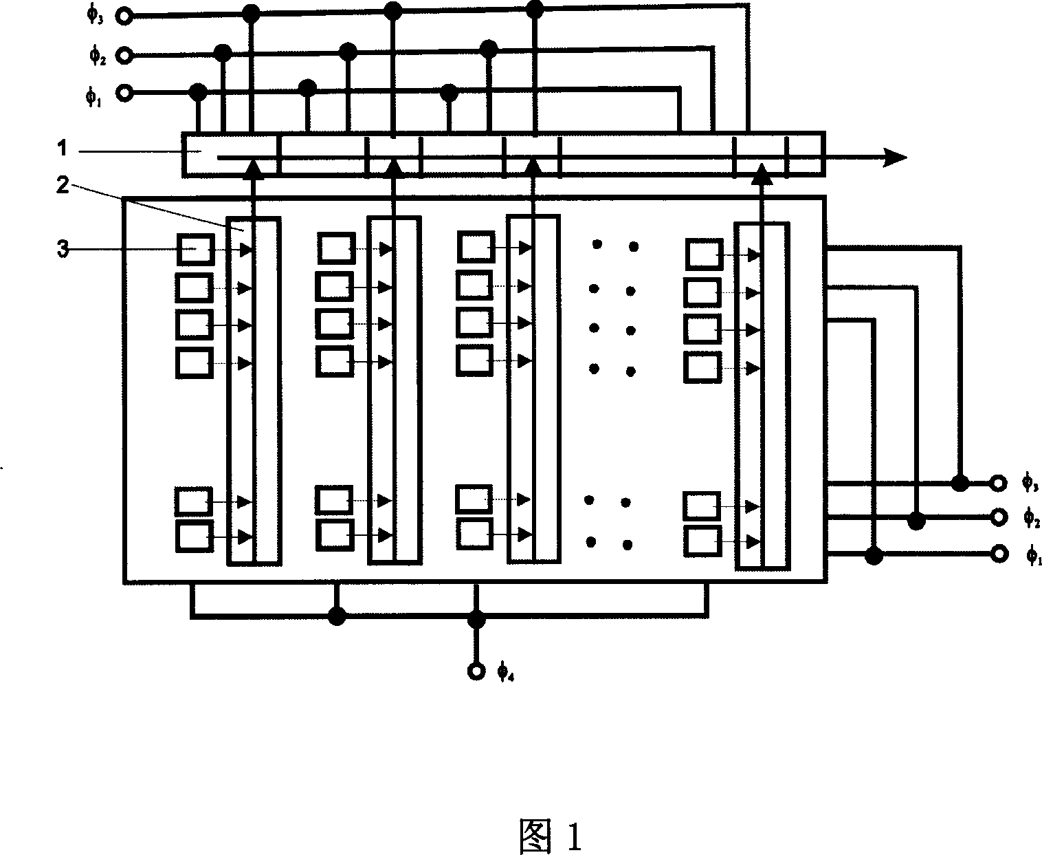
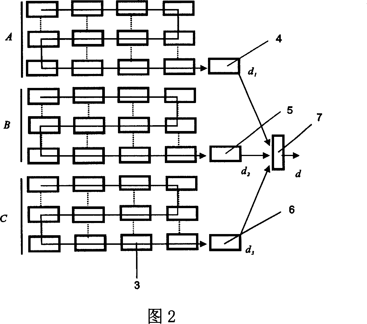
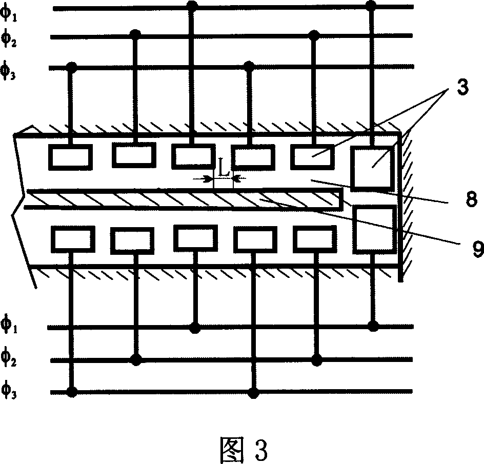
[0028] The area array CCD structure is to oxidize and grow a layer of SiO on the P-type silicon substrate 13 2 insulating layer 10, in SiO 2 The aluminum gate electrode 3 of the MOS photosensitive unit is fabricated by the overlapping gate process on the insulating layer 10, and the aluminum gate electrode 3 of the MOS photosensitive unit is pressurized to form a MOS capacitor potential well 11, and the photogenerated signal electrons 12 are inside the MOS capacitor potential well 11.

[0029] Figure 1 shows an existing three-phase interrow transfer area CCD structure. The aluminum gate electrode 3 of the MOS photosensitive unit forms the photosensitive area, and the transfer gate area is between the photosensitive area and the vertical transfer analog shift register 2. In the device In each column, the photosensitive area, the transfer gate...


PUM


Abstract

The invention relates to a charge-coupled device CCD, which comprises: P-type silicon liner, SiO2 insulated layer, and MOS light-sensitive aluminum grid electrode above the SiO2 insulated layer and the MOS light-sensitive unit aluminum grid electrodes with same number as phases, to form one working unit; the working units are transversely periodically arranged; and the MOS light-sensitive aluminum grid electrodes have groove between, while the electrodes of each row are separated by groove resistance; based on working impulse, the array is divided into several areas; the end of each area has float grid output amplifier; the outputs of each area are connected. The invention combines the light-sensitive area, transfer grid area and the analogue shift register, to be completed by three working steps, to simplify the structure, improve the resolution, improve detecting sensitivity and improve the output speed.

Description

technical field [0001] The invention belongs to the technical field of optical image data processing, and relates to an area array charge coupled device, in particular to an area array charge coupled device CCD adopting a detour transfer method. Background technique [0002] CCD (Charge Coupled Device) works by relying on the depletion layer coupling between highly integrated discrete MOS capacitors. The signal charge packet is transferred from the original position to the output port after the light accumulation is completed through the control of the gate voltage. The readout circuit converts one-dimensional or two-dimensional image information into a one-dimensional function of time to complete image acquisition. [0003] The interline transfer type, frame field transfer type, and vertical line type area array CCDs that have been developed so far, their working principles are described in "Application of Charge Coupled Devices in Signal Processing and Image Sensing" edite...

Claims


Application Information

Patent Timeline
Patent Type & Authority Applications(China)
IPC IPC(8): H01L27/148
Inventor 独育飞唐远河刘锴宁辉张磊李皓伟
Owner XIAN UNIV OF TECH
Why Eureka
Try Eureka