
Improved permalloy sensor

一种坡莫合金、传感器的技术,应用在磁场控制的电阻器、仪器、测量磁变量等方向,能够解决限制等问题,达到增加灵敏度、扩展感测范围的效果

Inactive Publication Date: 2007-04-25
HONEYWELL INT INC
View PDF2 Cites 0 Cited by
  • Summary
  • Abstract
  • Description
  • Claims
  • Application Information

AI Technical Summary

Problems solved by technology

However, permalloy runners such as those disclosed in the above-cited patents are all parallel to the direction of wafer-level anisotropy, the easy axis.
Therefore, they are limited in application by the strength of the magnetic field that can be sensed

Method used


Image

  • Improved permalloy sensor
  • Improved permalloy sensor

Examples


Embodiment Construction

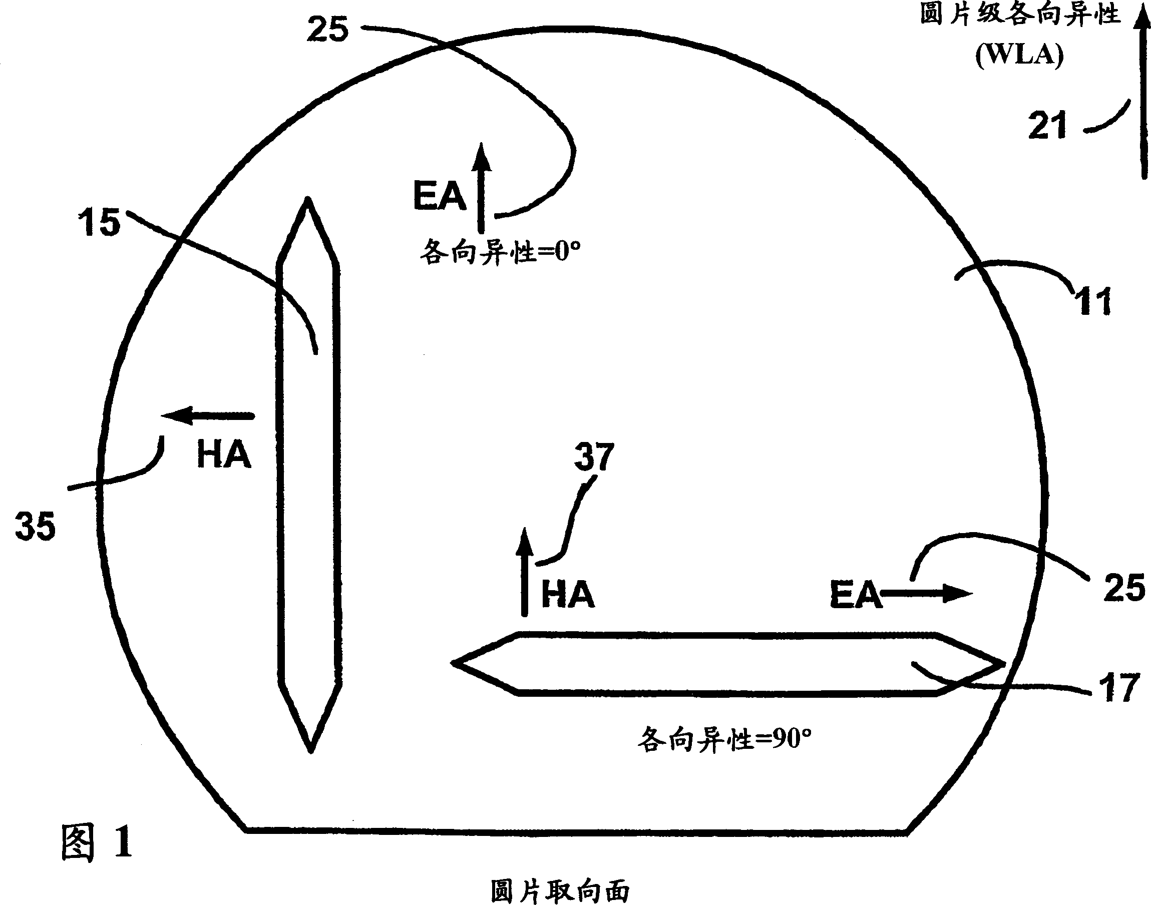
[0013] Referring to Figure 1, it should be understood that there may actually be thousands of permalloy deposits on a wafer, of which only two are shown for illustration. This is conventional in sputtering techniques, by using permanent magnets to bias the magnetic permalloy particles into alignment of the particles as they land on the substrate. This allows many permalloy resistors to be deposited and aligned in one direction. Also, when the resistors are deposited, they all have the same general orientation. Figure 1 is purely for illustration purposes.

[0014] In Figure 1, wafer 11 is shown having two different permalloy resistors 15 and 17 deposited thereon. In practice, the aspect ratio of permalloy resistors is very large, on the order of 100 or more, so permalloy resistors 15 and 17 are only schematic, as lines 100 times longer than their width cannot be clearly used as illustrate. The easy axis EA is always in the length direction of the resistor, so that permallo...


PUM


Abstract

A permalloy sensor having high sensitivity is presented. A substrate and a sensor has a first surface having a wafer level anisotropy in a given direction. A permalloy resistor pattern of individual runners is deposited on the surface such that the mechanical length of each of said individual runners is perpendicular to the wafer level anisotropy to cause the sensor to have an anisotropy of about 90 DEG. The permalloy is deposited as a thin film and a silicon wafer is the preferred substrate.

Description

technical field [0001] The present invention relates generally to magnetic films, and more particularly, to permalloy films having increased sensitivity in weak magnetic field applications. Background technique [0002] Thin-film magnetic devices are important to the storage industry, such as hard disk drive read heads, and magnetic sensors. In weak field applications, such as ring magnets, their functionality is limited by the lowest magnetic field strength that can be sensed. [0003] One specific technology where permalloy is well utilized is in magnetoresistive bridge arrays, as shown in US Patent No. 6,297,628. In this patent, a permalloy runner is formed in a conventional manner, as shown in commonly owned US Patent No. 5,667,879. [0004] Permalloy runners are formed in the above-cited patents to use an "easy" shaft. In the prior art, the permalloy runner lengths are cut in the anisotropic direction at the wafer level. This axis is called the "easy" axis. The eas...

Claims


Application Information

Patent Timeline
Patent Type & Authority Applications(China)
IPC IPC(8): G01R33/09H01L43/08H10N50/10
CPCH01L43/08H10N50/10
Inventor J·M·奇科特P·A·霍曼
Owner HONEYWELL INT INC
Learn More