
Optical semiconductor apparatus with clamped carrier density

A technology of semiconductors and optical amplifiers, which is applied in the fields of semiconductor lasers, semiconductor amplifier structures, laser components, etc., and can solve problems such as crosstalk and channel interference.

Inactive Publication Date: 2007-05-09
ALCATEL LUCENT SAS
View PDF0 Cites 2 Cited by
  • Summary
  • Abstract
  • Description
  • Claims
  • Application Information

AI Technical Summary

Problems solved by technology

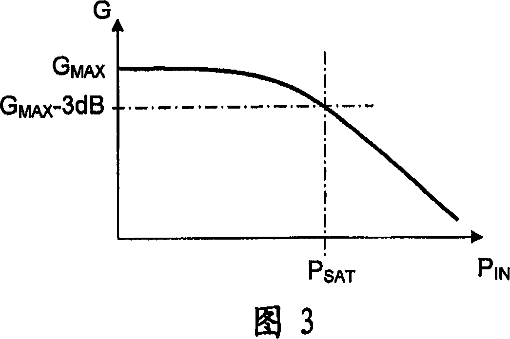
[0010] It has also been proven that if multiple optical channels modulated at different wavelengths are simultaneously amplified, interference or crosstalk will occur between the channels

Method used


Image

  • Optical semiconductor apparatus with clamped carrier density
  • Optical semiconductor apparatus with clamped carrier density
  • Optical semiconductor apparatus with clamped carrier density

Examples


Embodiment Construction

[0033] Quantum dots are microstructures containing small amounts of charge carriers, free electrons or holes. They are fabricated in semiconductor-type materials and have dimensions between a few nanometers and tens of nanometers in three dimensions. In this way, the size and shape of these structures and thus the number of cavities they contain can be precisely controlled. Quantifying energy levels in quantum dots, just as in atoms, makes these structures particularly favorable for a large number of physical applications.

[0034] As shown in Figure 8, there are only two possible energy transition states in the quantum dot structure, which are called the ground state (GS) and the excited state (ES), and the ground state corresponds to the lowest energy level. These two transition states correspond to the two vertical arrows shown in Fig. 8. Corresponding to these two transition states are two emission wavelengths, given by λ ES and lambda GS express. As already mentioned...


PUM


Abstract

The field of the invention is that of semiconductor devices used for the amplification or for the phase modulation of optical signals. These devices are known by the generic names SOA (semiconductor optical amplifier) and DPSK (differential phase shift keying) modulators. The main drawbacks of this type of device are that it is, on the one hand, difficult to obtain a constant gain, and, on the other hand, it is difficult for the optical signal to be independently amplitude-modulated and phase-modulated. The device according to the invention does not have these drawbacks. It relies essentially on three principles: the active zone of the device has a quantum dot structure, the atoms of said structure possessing a first energy transition state called the ground state and a second energy transition state called the excited state; the active zone is placed in a structured resonant cavity in order to resonate at a first wavelength corresponding to the ground state; and the current flowing through the active zone is greater than the saturation current of the ground state so as to allow oscillation at a second wavelength corresponding to the excited state.

Description

technical field [0001] The field of the invention is that of semiconductor devices for optical signal amplification or phase modulation. Devices used for amplification are collectively referred to under the general name SOA (Semiconductor Optical Amplifier). Background technique [0002] Current semiconductor devices used for optical signal amplification or modulation have several disadvantages. [0003] First, changes in the optical gain of an active medium are inherently associated with changes in the optical index of the active medium, that is, changes in the gain cause changes in the amplitude of the optical signal, while changes in the optical index cause changes in the phase. In these cases it is not possible to obtain independently amplitude and phase modulated signals. This phenomenon can significantly degrade the performance of a DPSK or DOPSK type optical modulator. [0004] Second, optical amplifying devices have significant disadvantages. When the power of th...

Claims


Application Information

Patent Timeline
Patent Type & Authority Applications(China)
IPC IPC(8): G02F3/00G02F2/00H01S5/00H01S5/12
CPCH01S5/12H01S5/50H01S5/341H01S5/5072B82Y20/00
Inventor 贝亚特丽斯·达让斯
Owner ALCATEL LUCENT SAS
Learn More