Photodetectors and optically pumped emitters based on III-nitride multiple-quantum-well structures

a technology of iiinitride and emitter, which is applied in the direction of semiconductor devices, electrical devices, nanotechnology, etc., can solve the problems of limited quantum efficiency and response speed of bulk-based photodetectors, and achieve the effect of reducing the number of iiinitride atoms, and improving the quality of iiinitride atoms

Inactive Publication Date: 2004-07-15
RES FOUND THE CITY UNIV OF NEW YORK
View PDF5 Cites 46 Cited by
  • Summary
  • Abstract
  • Description
  • Claims
  • Application Information

AI Technical Summary

Problems solved by technology

However, quantum efficiency and response speed of bulk-based photodetectors

Method used


Image

  • Photodetectors and optically pumped emitters based on III-nitride multiple-quantum-well structures
  • Photodetectors and optically pumped emitters based on III-nitride multiple-quantum-well structures
  • Photodetectors and optically pumped emitters based on III-nitride multiple-quantum-well structures

Examples


Embodiment Construction

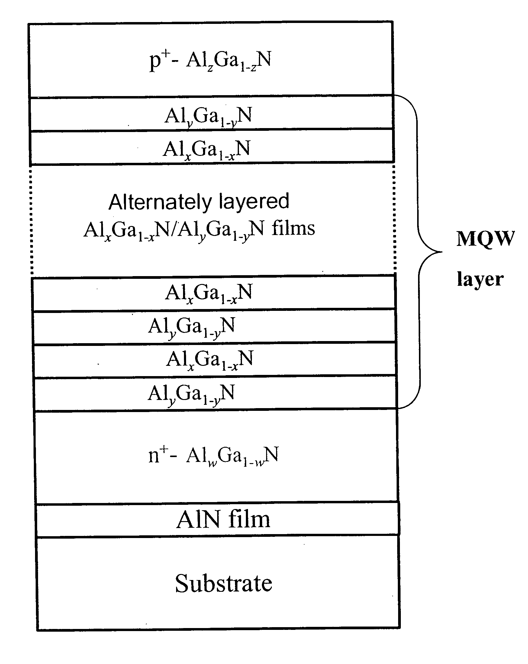
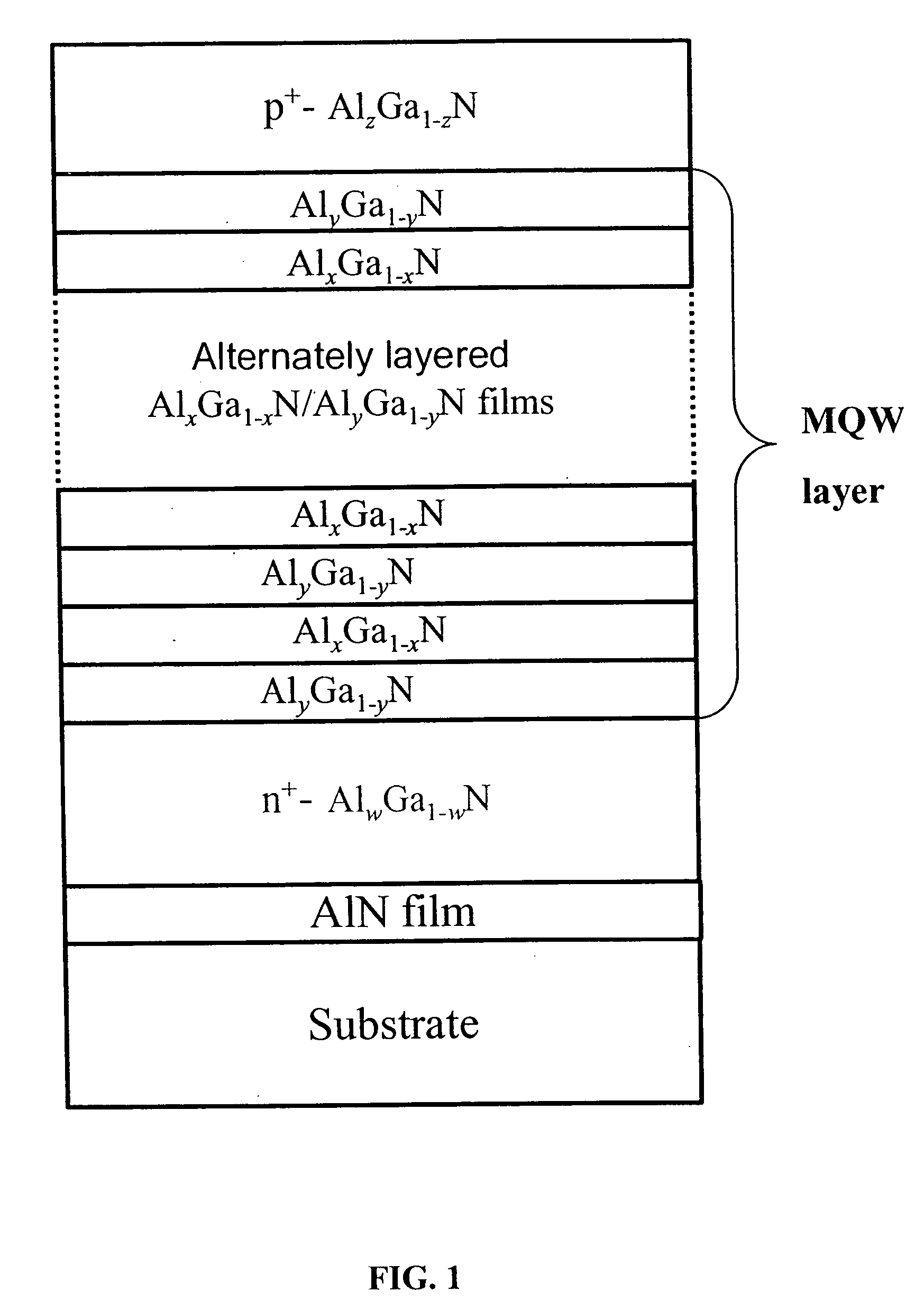
[0029] All materials of III-nitride compound semiconductors are utilizable in the design of photodetectors and emitters according to the present invention. AlGaN alloys are used in the following examples as being representative.

[0030] Layered Semiconductor Structure of a Photodetector

[0031] Referring to FIG. 1, a layered semiconductor structure of a photodetector based on Al.sub.xGa.sub.1-xN / Al.sub.yGa.sub.1-yN (x


PUM


Abstract

The design and operation of a p-i-n device, operating in a sequential resonant tunneling condition for use as a photodetector and an optically pumped emitter, is disclosed. The device contains III-nitride multiple-quantum-well (MQW) layers grown between a III-nitride p-n junction. Transparent ohmic contacts are made on both p and n sides. The device operates under a certain electrical bias that makes the energy level of the first excitation state in each well layer correspond with the energy level of the ground state in the adjoining well layer. The device works as a high-efficiency and high-speed photodetector with photo-generated carriers transported through the active MQW region by sequential resonant tunneling. In a sequential resonant tunneling condition, the device also works as an optically pumped infrared emitter that emits infrared photons with energy equal to the energy difference between the first excitation state and the ground state in the MQWs.

Description

[0001] This application claims priority from U.S. Provisional Patent Application Serial No. 60 / 430,971 which was filed on Dec. 5, 2002.[0002] 1. Field of the Invention[0003] This invention relates to sequential resonant tunneling (SRT) photodetector and emitter devices based on III-nitride multiple-quantum-well (MQW) structures; to methods of their fabrication; and to methods of their use, where III-nitride refers to compound alloys of nitride and group III elements including aluminum, gallium, and indium.[0004] 2. Description of the Related Art[0005] III-nitride-based photodetectors are used in space-to-earth and space-to-space communication, missile plume detection, detection of biological organisms and bacteria, combustion sensing and control for aircraft engines, optical storage, air quality monitoring, cancer diagnosis, and personal ultraviolet exposure dosimetry. Alloys of III-nitride are becoming the semiconductor of choice for photodetectors and light emitters in the wavelen...

Claims


Application Information

Patent Timeline
IPC IPC(8): H01L31/075H01L33/00H01L33/06
CPCB82Y10/00B82Y20/00H01L33/06H01L31/1035H01L33/0012H01L31/035236Y02E10/548
Inventor ALFANO, ROBERT R.ZHANG, SHENGKUNWANG, WUBAO
Owner RES FOUND THE CITY UNIV OF NEW YORK
Why Eureka
Try Eureka