Dual welding spots inductor in high frequency packaged by ceramics
A technology of ceramic packaging and inductors, which is used in the manufacture of inductors/transformers/magnets, transformer/inductor housings, inductors with magnetic cores, etc. or short circuit, etc., to achieve the effect of large inductance value, reduction of winding short circuit, and small size
- Summary
- Abstract
- Description
- Claims
- Application Information
AI Technical Summary
Problems solved by technology
Method used
Image
Examples
Embodiment Construction
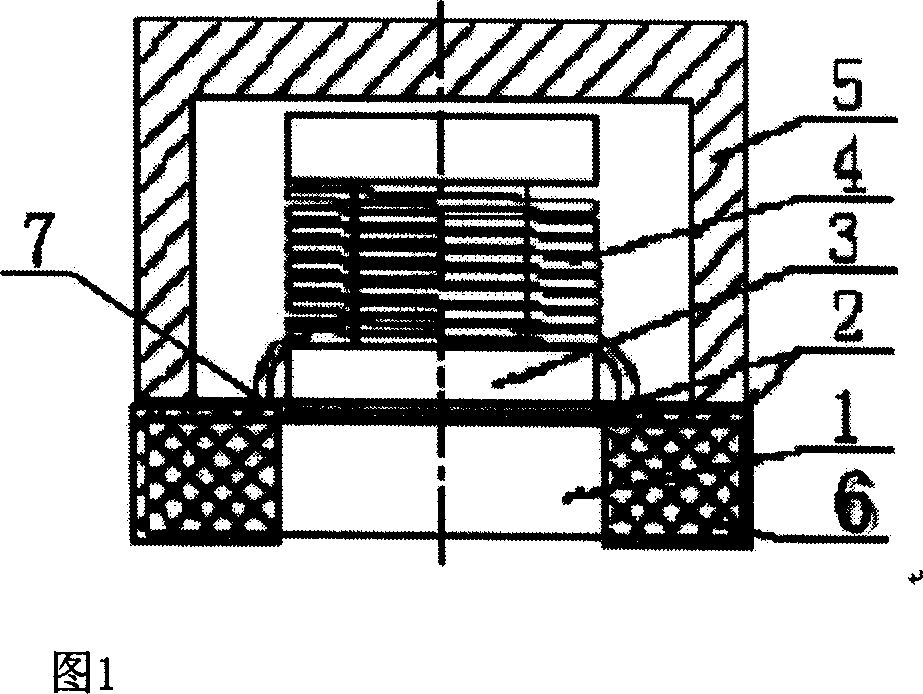
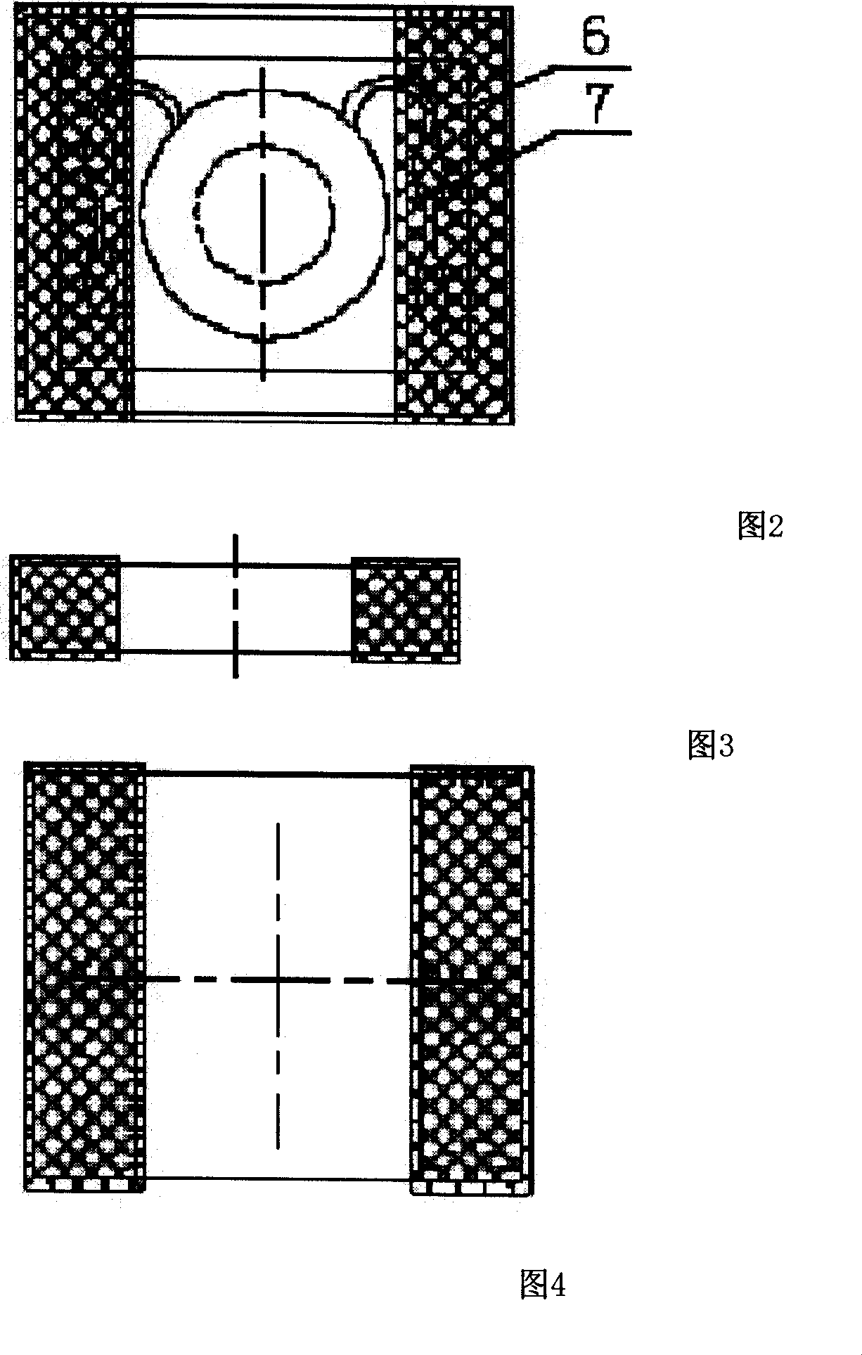
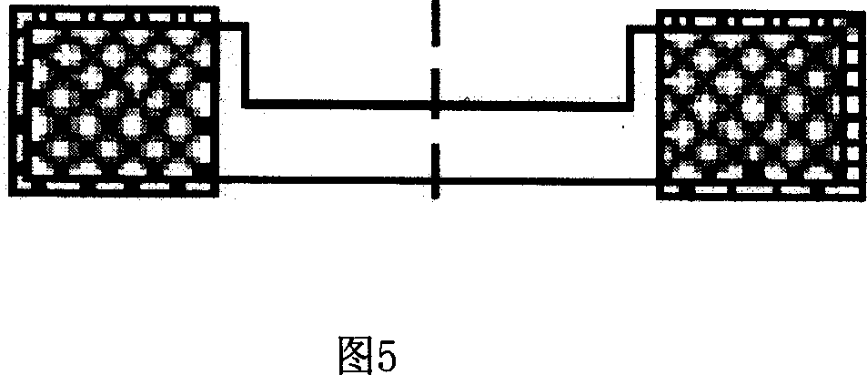
[0026] Embodiment of the present invention: as shown in Figures 1 and 2, at first the magnetic core 3 is fixed on the ceramic substrate 1 with the metal lead-out end with an adhesive 2, and all surfaces at both ends of the ceramic substrate 1 are electroplated to form a metal coating 6. It is preferably gold-plated or tin-plated, so that the ceramic substrate 1 becomes a simple but very practical conduction structure. Double-layer enameled wire 4 is used to wind on the magnetic core 3, and then the leading end is welded on the metal coating 6 of the ceramic substrate 1 by thermocompression welding to obtain double solder joints 7 and metal coating 6, so that the double-layer enameled wire 4 can be welded The point and the derived welding surface required by the user are effectively dispersed to avoid the occurrence of solder joint damage and failure when the product is soldered on the PCB board. The ceramic shell 5 and the ceramic substrate 1 are sealed and bonded with the adhe...
PUM
 Abstract
Description
Claims
Application Information


