Dual welding spots inductor in high frequency packaged by ceramics and its production method

A ceramic packaging and inductor technology, applied in the manufacture of inductors/transformers/magnets, transformer/inductor housings, inductors with magnetic cores, etc. Poor reliability and other problems, to achieve the effect of large inductance value, small size, and reducing the short circuit of the winding

Inactive Publication Date: 2011-04-27
VONTRON TECH CO LTD
View PDF0 Cites 0 Cited by
  • Summary
  • Abstract
  • Description
  • Claims
  • Application Information

AI Technical Summary

Problems solved by technology

[0002] The solder joints of the enameled wire of general high-frequency wound inductors are all single solder joints, and the solder joints and the derived welding surface required by the user are located on the same plane, and the solder joints are exposed to the external environment, which may easily lead to open circuit or short circuit , while the epoxy resin coating covering the enameled wire is only potted on the enameled wire, and only protects the enameled wire encapsulation
In addition, due to the difference in expansion coefficient between epoxy resin and enameled wire, working for a long time in an environment with alternating cold and heat or in a corrosive and humid environment will cause open or short circuits in the product, resulting in poor reliability of the inductor, and cannot meet the needs of contemporary people. high quality high quality requirements

Method used


Image

  • Dual welding spots inductor in high frequency packaged by ceramics and its production method
  • Dual welding spots inductor in high frequency packaged by ceramics and its production method
  • Dual welding spots inductor in high frequency packaged by ceramics and its production method

Examples


Embodiment Construction

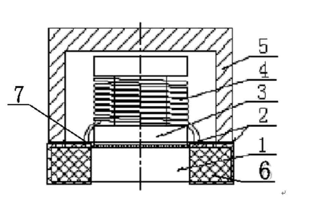
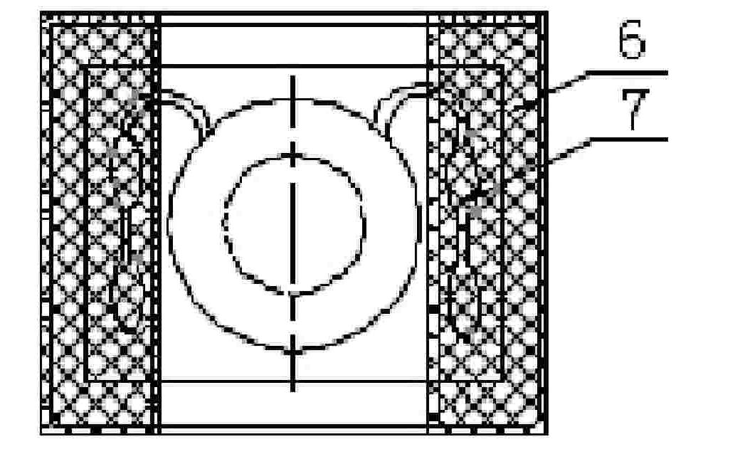
[0026] Embodiments of the invention: as figure 1 with 2 As shown, at first the magnetic core 3 is fixed on the ceramic substrate 1 with the metal lead-out end with an adhesive 2, and all surfaces at both ends of the ceramic substrate 1 are electroplated to form a metal coating 6, preferably gold-plated or tin-plated, so The ceramic substrate 1 becomes a simple but very practical conduction structure. Double-layer enameled wire 4 is used to wind on the magnetic core 3, and then the leading end is welded on the metal coating 6 of the ceramic substrate 1 by thermocompression welding to obtain double solder joints 7 and metal coating 6, so that the double-layer enameled wire 4 can be welded The point and the derived welding surface required by the user are effectively dispersed to avoid the occurrence of solder joint damage and failure when the product is soldered on the PCB board. The ceramic shell 5 and the ceramic substrate 1 are sealed and bonded with the adhesive 2 , the ma...


PUM


Abstract

Method for manufacturing the disclosed inductor in high frequency includes steps: fixing up magnetic core on the ceramic base plate with leading out ends of metal; next, winding double lacquered wires on magnetic core; then, soldering double lacquered wires on leading out ends of metal so as to form duplex soldered points; finally, using ceramic package to enclosure protect to protect double lacquered wires and soldered points. Features are: reasonable design configuration, small size, large value of inductance, and high Q value. Being suitable to electronic products stuck assembled in high density and in mini type. Being reached to astronavigation level, the product possesses high reliability.

Description

technical field [0001] The invention relates to a high-frequency inductor and a manufacturing method thereof, in particular to a high-frequency inductor with a double solder joint ceramic package and a manufacturing method thereof. Background technique [0002] The solder joints of the enameled wire of general high-frequency wound inductors are all single solder joints, and the solder joints and the derived welding surface required by the user are located on the same plane, and the solder joints are exposed to the external environment, which may easily lead to open circuit or short circuit , while the epoxy resin coating covering the enameled wire is only potted on the enameled wire, and only protects the enameled wire package. In addition, due to the difference in expansion coefficient between epoxy resin and enameled wire, working for a long time in an environment with alternating cold and heat or in a corrosive and humid environment will cause open or short circuits in th...

Claims


Application Information

Patent Timeline
Patent Type & Authority Patents(China)
IPC IPC(8): H01F17/04H01F27/02H01F41/00
Inventor 高海明戴正立李青彭兰波
Owner VONTRON TECH CO LTD
Why Eureka
Try Eureka