Wet process device for etching wafer, and wet process etching method

A wet etching and wafer technology, which is applied in the direction of electrical components, semiconductor/solid-state device manufacturing, circuits, etc., can solve the problems of uneven etching on the wafer surface, lower process accuracy, and affect product yield, etc.

Inactive Publication Date: 2007-05-09
MACRONIX INT CO LTD
View PDF0 Cites 10 Cited by
  • Summary
  • Abstract
  • Description
  • Claims
  • Application Information

AI Technical Summary

Problems solved by technology

In turn, the phenomenon of uneven etching on the surface of the wafer occurs...

Method used


Image

  • Wet process device for etching wafer, and wet process etching method
  • Wet process device for etching wafer, and wet process etching method
  • Wet process device for etching wafer, and wet process etching method

Examples


Embodiment Construction

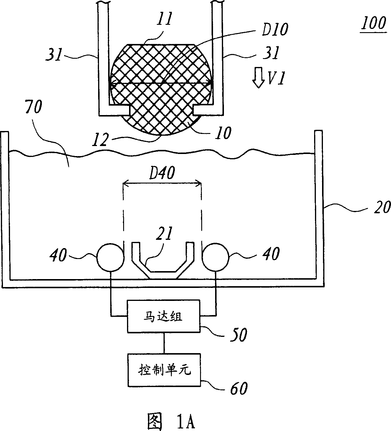
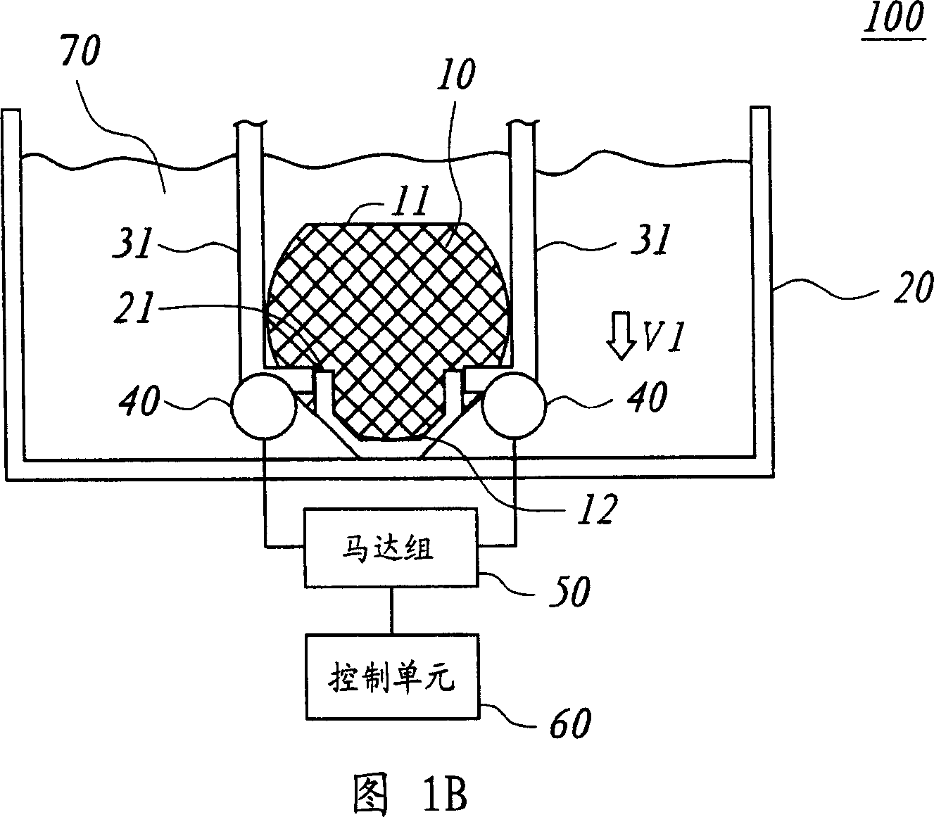
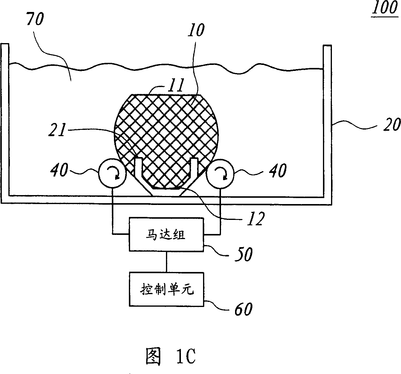
[0035] Please refer to FIGS. 1A-1E and FIG. 2 at the same time. FIGS. 1A-1E are schematic diagrams of a wafer wet etching device according to a wafer wet etching method according to a preferred embodiment of the present invention. FIG. 2 is a schematic diagram illustrating the orientation of the wafer and the spinner. The wafer wet etching device 100 includes an etching tank 20 , a clamp 31 and a rotating mechanism. The etching tank 20 is used for accommodating an etching solution 70, and the etching solution 70 can be an acidic solution or an alkaline solution. The clamp 31 is used for clamping a wafer 10 into and out of the etchant 70 . In this embodiment, the gripper 31 is described by taking a robot arm as an example. The rotating mechanism is disposed in the etching tank 20 for rotating the wafer 10 in the etching solution 70 . In this embodiment, the rotating mechanism is described by taking two rotating columns 40 as an example.

[0036] The two rotating columns 40 ...


PUM


Abstract

The invention is related to wet-process etching device for wafer, and wet-process etching method. The method includes following steps: first, placing a wafer to an etching fluid; then, rotating wafer in etching fluid.

Description

technical field [0001] The invention relates to a wafer wet etching device and a wet etching method thereof, in particular to a wafer wet etching device and a wet etching method for rotating a wafer in etching liquid. Background technique [0002] Electronic products are changing with each passing day. Along with the increasing demand for semiconductor chips, the rapid development of semiconductor technology has been driven. In order to reduce the volume occupied by the chip, the line width in the chip is continuously reduced. Therefore, the semiconductor process capability is severely tested, and the control of process accuracy and process variation is more important. Especially taking the wet etching process in the semiconductor process as an example, the variation of etching depth will greatly affect the yield rate of chip products. [0003] A conventional wafer wet etching method is to immerse a wafer in a wet etching solution, and the wet etching solution can perform ...

Claims


Application Information

Patent Timeline
IPC IPC(8): H01L21/306H01L21/311H01L21/3213H01L21/00
Inventor 彭国豪曾国邦
Owner MACRONIX INT CO LTD
Why Eureka
Try Eureka