

Method for etching through hole
A main etching and over-etching technology, used in electrical components, semiconductor/solid-state device manufacturing, circuits, etc., can solve problems such as large fluctuations in etching rate, unstable etching process, and reaction chamber pollution, and avoid Etching unevenness, reducing etch rate and increasing efficiency
- Summary
- Abstract
- Description
- Claims
- Application Information
AI Technical Summary
Problems solved by technology
Method used
Image

Examples
Embodiment Construction
[0034] Embodiments embodying the features and advantages of the present invention will be described in detail in the following description. It should be understood that the invention is capable of various changes in different examples without departing from the scope of the invention, and that the descriptions and illustrations therein are illustrative in nature rather than limiting the invention.
[0035] The etching method of the etching stop layer of the present invention can be adopted but not limited to the plasma etching method and applied in the plasma etching process chamber. In the present invention, the plasma process chamber can adopt any type, The present invention does not make any limitation thereto.
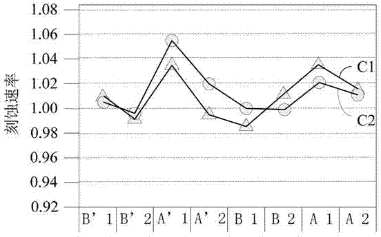
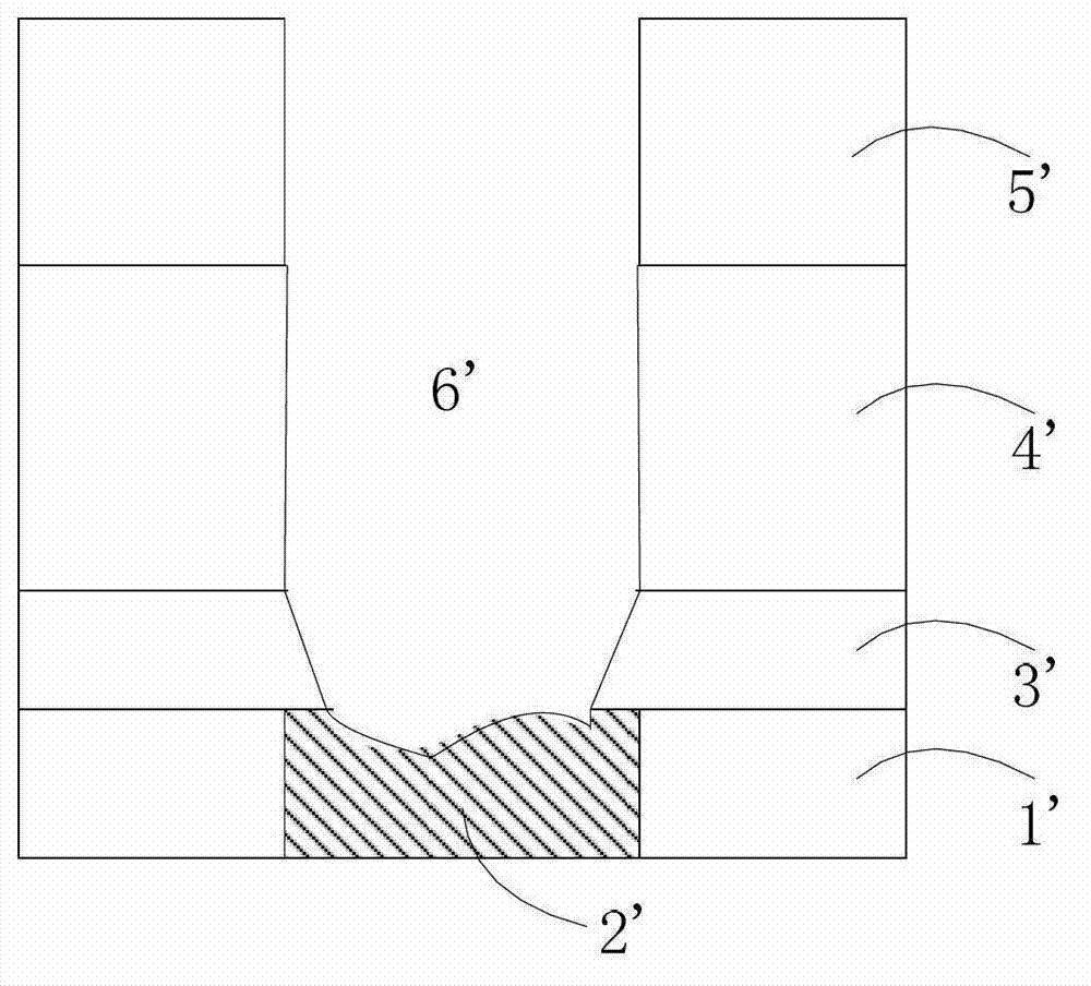
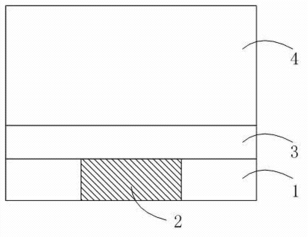
[0036] now attached Figure 2-6 , a through-hole etching method of the present invention will be further described in detail through specific embodiments. It should be noted that the drawings are all in a very simplified form, using imprecise scales, and are only...
PUM
 Abstract
Description
Claims
Application Information