

Liquid crystal display device
A technology of liquid crystal display device and liquid crystal layer, applied in static indicators, nonlinear optics, instruments, etc., can solve problems such as uniform orientation, difficult to obtain retardation, electrostatic damage, etc.
- Summary
- Abstract
- Description
- Claims
- Application Information
AI Technical Summary
Problems solved by technology
Method used
Image

Examples
Embodiment 1
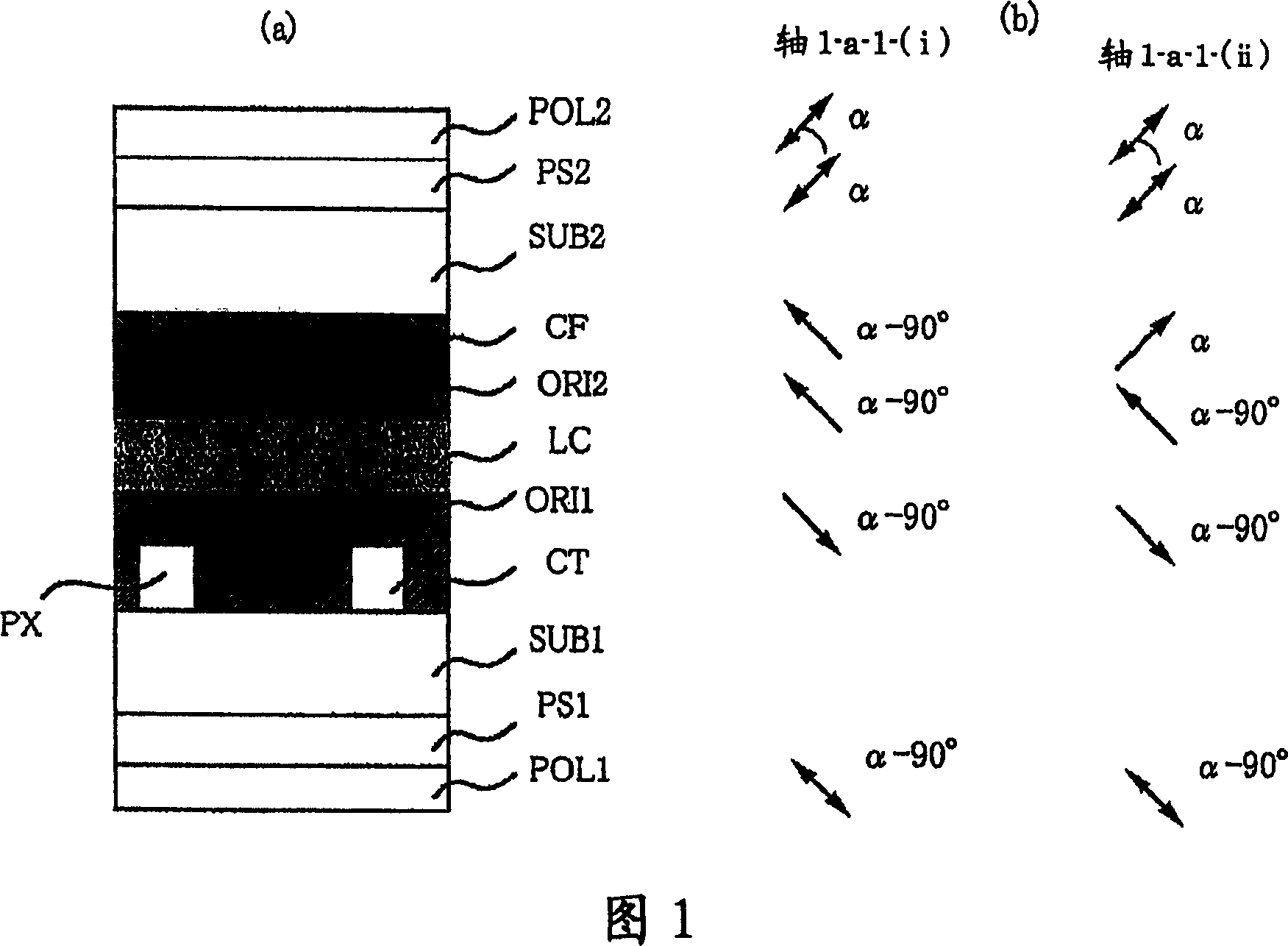
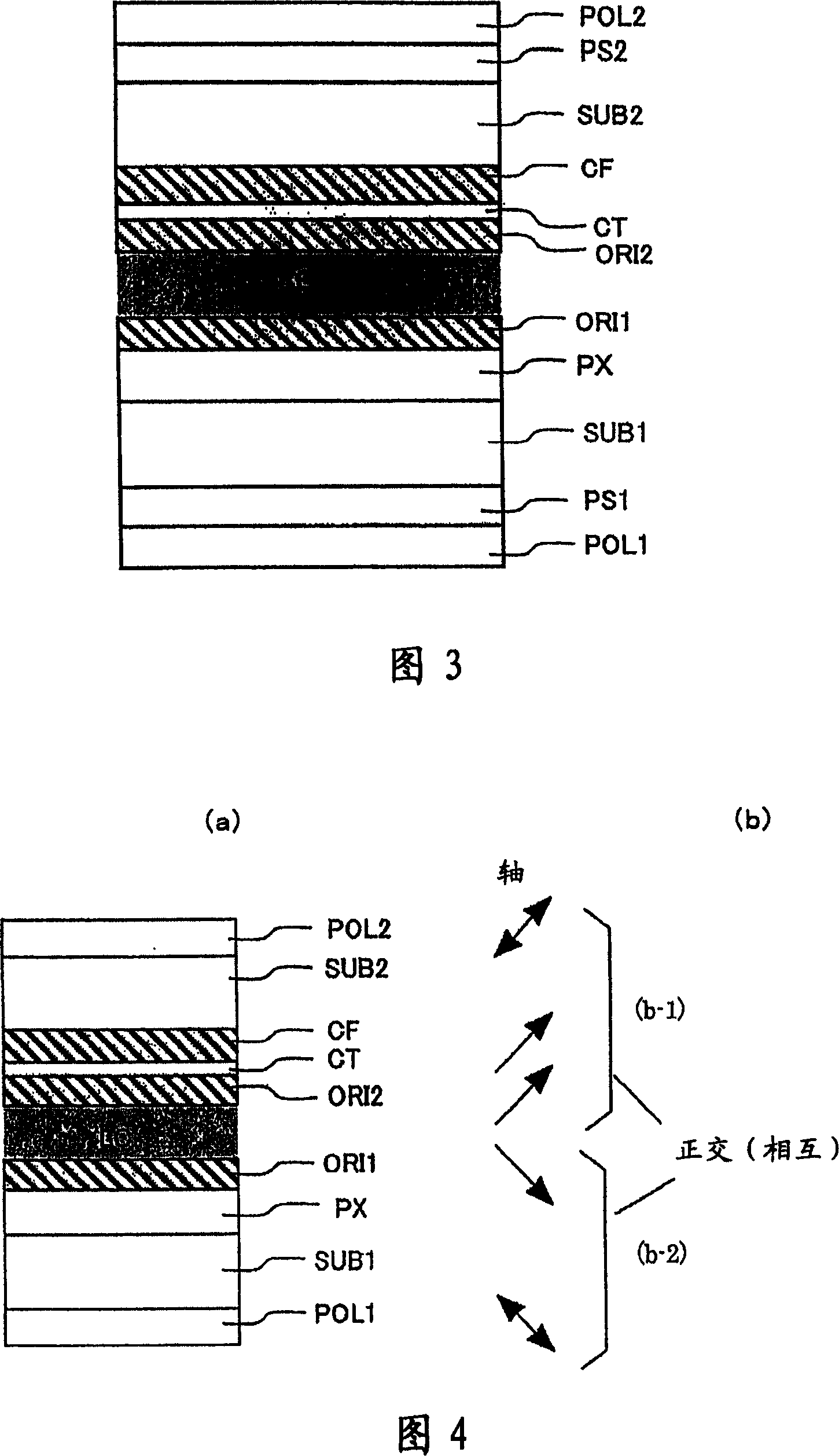
[0036]FIG. 1 is an explanatory diagram illustrating a cross-sectional structure and an axial structure of an IPS mode liquid crystal panel according to Embodiment 1 of the present invention. (a) of Fig. 1 is a cross-sectional structure diagram of a liquid crystal panel constituting an IPS liquid crystal display device, a liquid crystal layer LC is sandwiched between substrates SUB1 and SUB2, and an organic material such as a color filter CF is arranged on the main surface of a substrate SUB2. An orientation film ORI2 is arranged on the color filter CF. In addition, the pixel electrode PX and the counter electrode CT are arranged on the main surface of the substrate SUB1, and the orientation film ORI1 is arranged thereon.
[0037] FIG. 1( b ) is an explanatory diagram of the axial structure of the IPS liquid crystal panel shown in FIG. 1( a ). In addition, α in (b) of FIG. 1 is an arbitrary angle of 0 to 360°. In addition, the direction of the axis is a direction indicating t...
Embodiment 2
[0101] In Example 1, for the substrate SUB2 on which the organic film such as the color filter CF is formed, and the substrate SUB1 on which the pixel electrode PX and the counter electrode CT are formed, polyimide is coated on these substrates by the spin coating method. A 6% N-methylpyrrolidone solution of acid and polyimide is heat-treated at 230° C. for 2 hours to form an alignment film layer OR12 or OR11 with a film thickness of about 100 nm. In the alignment treatment of the alignment film, the wavelength of 254nm is used, and the converted value is about 15mW / cm 2 The polarized light irradiation system with the highest light intensity, adjust the irradiation time so that the irradiation amount is 20J / cm 2 irradiate the linearly polarized light. In addition, at the time of irradiation, the substrate was placed on a hot plate that can be heated to 150° C., and irradiation was performed while heating. The manufacturing method of other liquid crystal display devices is th...
Embodiment 3
[0104] In Example 1, the substrate SUB2 on which the organic film such as the color filter CF is formed, and the substrate SUB1 on which the pixel electrode PX and the counter electrode CT are formed are coated with polyimide by the spin coating method. The 8% N-methylpyrrolidone solution of acid and polyimide is heat-treated at 230° C. for 2 hours to form an alignment film layer OR12 or OR11 with a film thickness of about 200 nm. In the alignment treatment of the alignment film, the wavelength of 254nm is used, and the converted value is about 15mW / cm 2 The polarized light irradiation system with the highest light intensity, adjust the irradiation time so that the irradiation amount is 15J / cm 2 irradiate the linearly polarized light. In addition, at the time of irradiation, the substrate was placed on a hot plate that can be heated to 200° C., and irradiation was performed while heating. The manufacturing method of other liquid crystal display devices is the same as that of...
PUM
 Abstract
Description
Claims
Application Information