Electroluminescence display device and its detection method

A technology of a display device and an inspection method, applied in the fields of EL display panels, information displays and the like, can solve problems such as irregularities in transistor display

Inactive Publication Date: 2007-05-30
JAPAN DISPLAY CENTRAL CO LTD
View PDF1 Cites 18 Cited by
  • Summary
  • Abstract
  • Description
  • Claims
  • Application Information

AI Technical Summary

Problems solved by technology

However, since organic EL elements emit light using electric current, there is a p

Method used


Image

  • Electroluminescence display device and its detection method
  • Electroluminescence display device and its detection method
  • Electroluminescence display device and its detection method

Examples


Embodiment Construction

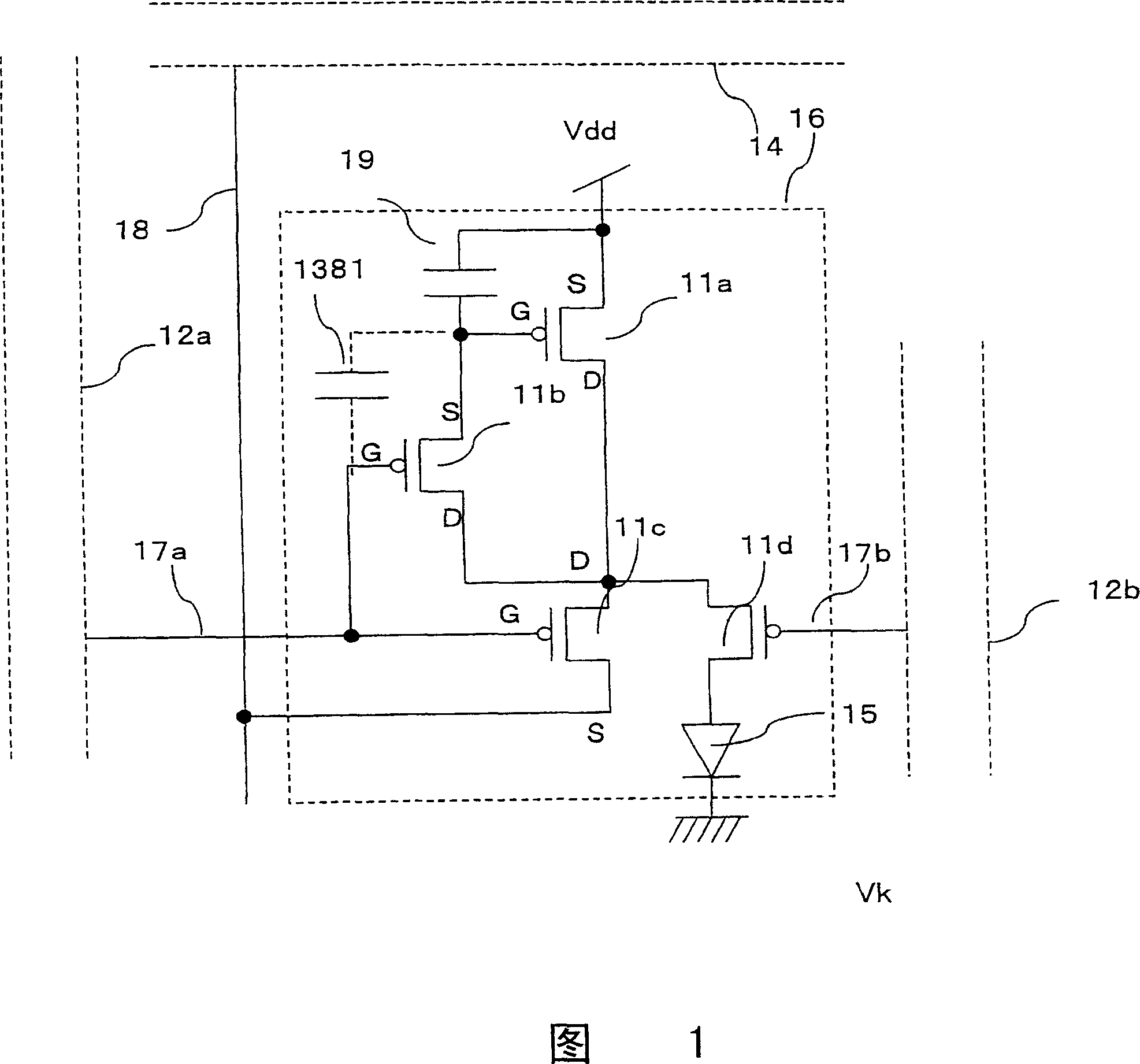
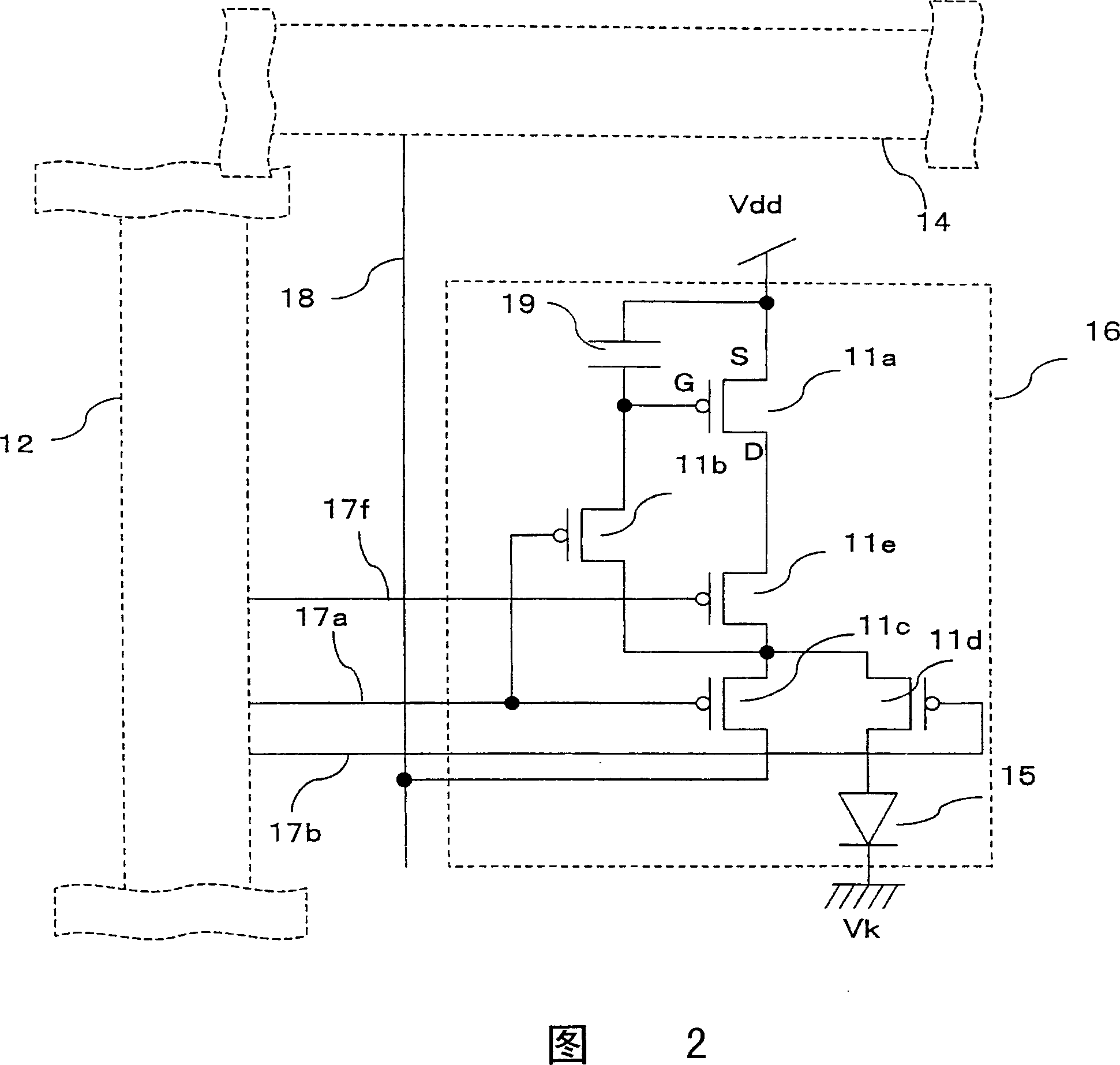
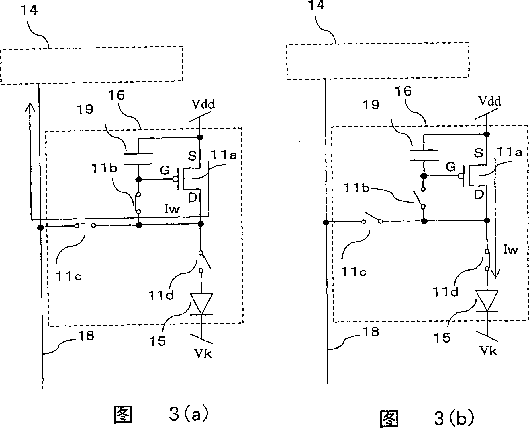
[0417] Some parts of the drawings are omitted and / or enlarged / reduced for convenience of understanding and / or illustration. For example, in the sectional view of the display panel shown in FIG. 11 , the packaging film 111 and the like shown are considerably thick. On the other hand, in Fig. 10, the sealing cap 85 is shown to be relatively thin. Some parts are omitted. For example, although the display panel according to the present invention requires a polarizing plate (such as a circular polarizing plate) having a phase film to prevent reflection, the phase film is omitted in the drawings here. This also applies to the figures below. In addition, the same or similar shapes, materials, functions or operations are denoted by the same reference numerals or characters.

[0418]Incidentally, the contents described with reference to the drawings and the like can be combined with other examples and the like even if not explicitly noted. For example, in FIG. 8, a touch panel or t...


PUM


Abstract

In order to adequately charge/discharging a parasitical capacitor of a source signal line and program a predetermined current value to a pixel transistor, a relative large current must be outputted from a source excited circuit. However, if a so large current flows through the source signal line, the current value is programmed into pixels, that induces a current large than a needed current passed through an EL component 15. For example, if programing is performed by using a 10 times current, the 10 times current flows through the EL component 15 so that the EL component 15 is lighted with a 10 times lightness. The time for current flowing through the EL component is reduced to 1/10 of a frame (1F) to obtain a predetermined transmitting lightness.

Description

[0001] This application is a divisional application of the parent application with the title of invention "Excitation Method for EL Display Panel", the filing date is March 6, 2003, and the application number is 03815038.7 (PCT / JP03 / 02597). technical field [0002] The present invention relates to a self-luminous display panel, such as an EL display panel using organic or inorganic electroluminescent (EL) elements. Also, it relates to information displays and the like, which use EL display panels, a driving method for the EL display panel, and a driving circuit for the EL display panel. Background technique [0003] In general, an active matrix display displays images by arranging a large number of pixels in a matrix and controlling the light intensity of each pixel corresponding to a video signal. For example, if liquid crystal is used as the electrochemical substance, the transmittance of each pixel changes according to the voltage written to the pixel. Even in the case o...

Claims


Application Information

Patent Timeline
IPC IPC(8): G09G3/30G09G3/32G09G3/20G09G3/00G01R31/00G01R19/00H05B33/08H05B33/14H05B37/02H01L51/50H01L27/32G09F9/33G09G3/3225H05B44/00
CPCY02B20/325
Inventor 高原博司柘植仁志
Owner JAPAN DISPLAY CENTRAL CO LTD
Why Eureka
Try Eureka