Array substrate for X-ray detector and X-ray detector comprising the same

a technology of array substrate and x-ray detector, which is applied in the direction of semiconductor/solid-state device testing/measurement, radiofrequency control devices, instruments, etc., can solve the problems of lowering the accuracy of test, and difficulty in evaluating the unique characteristics of each of thin film transistors and optical diodes, and achieves high accuracy

Active Publication Date: 2018-09-25
LG DISPLAY CO LTD
View PDF8 Cites 0 Cited by
  • Summary
  • Abstract
  • Description
  • Claims
  • Application Information

AI Technical Summary

Benefits of technology

[0010]It is an object of the present disclosure to provide an array substrate for an X-ray detector for capable of separately measuring characteristics of a transistor and an optical detector of the X-ray detector with a high accuracy.

Problems solved by technology

In this regard, there is a problem in that a cesium component corrodes metallic lines of the array substrate 1 of a thin film transistor, and thus an uppermost layer of the active area of the array substrate is typically protected by an organic layer.
However, the test pattern added to the edge portion of the sheet material of the base substrate is distant from the active area of the array substrate, and thus the accuracy of the test is lowered.
Accordingly, it is difficult to evaluate unique characteristics of each of the thin film transistor and optical diode.

Method used


Image

  • Array substrate for X-ray detector and X-ray detector comprising the same
  • Array substrate for X-ray detector and X-ray detector comprising the same
  • Array substrate for X-ray detector and X-ray detector comprising the same

Examples


Embodiment Construction

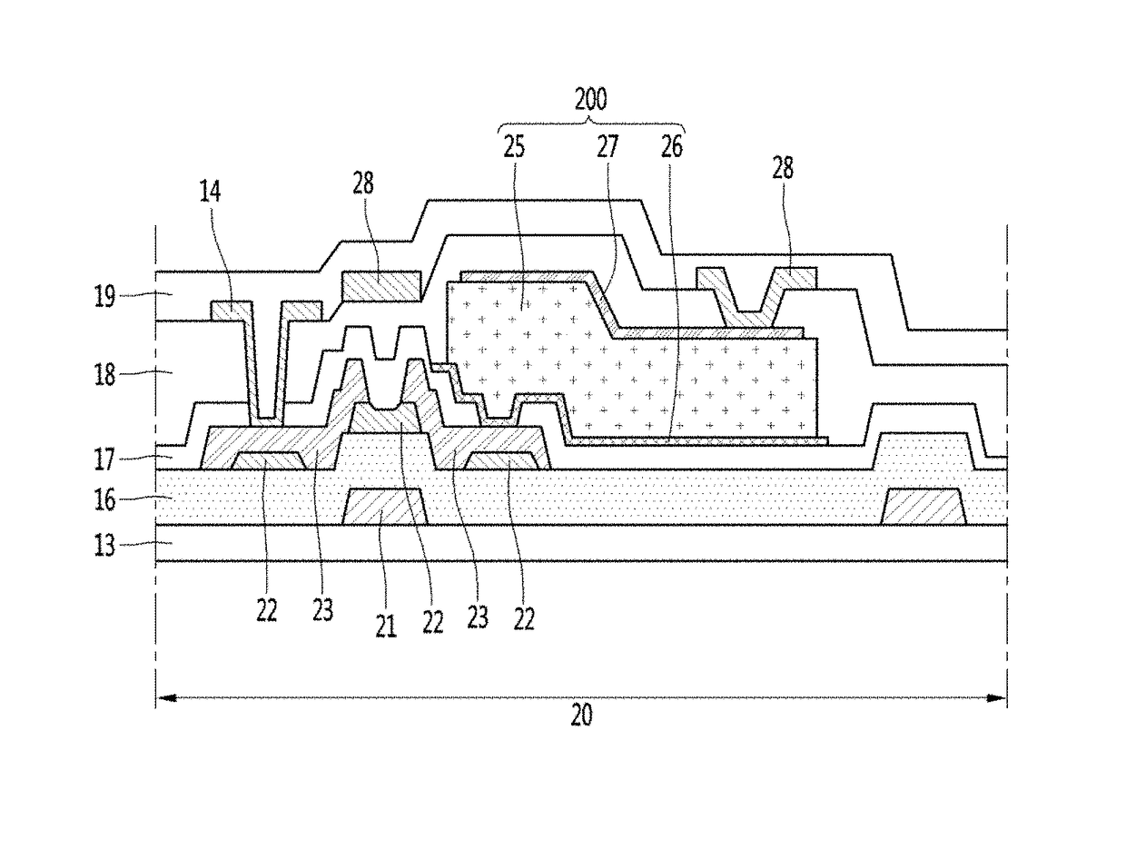
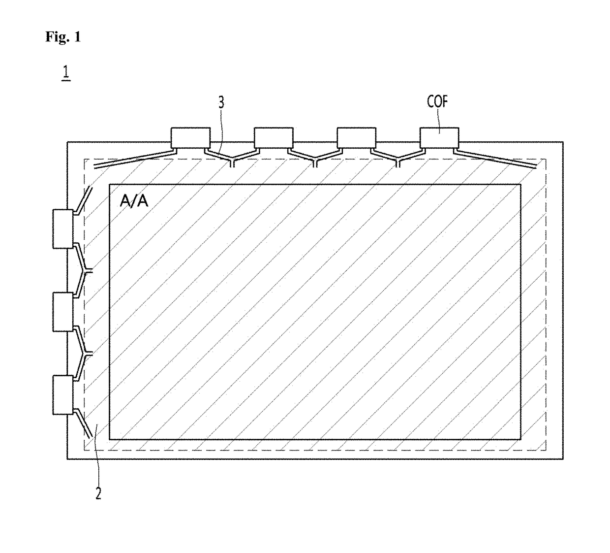
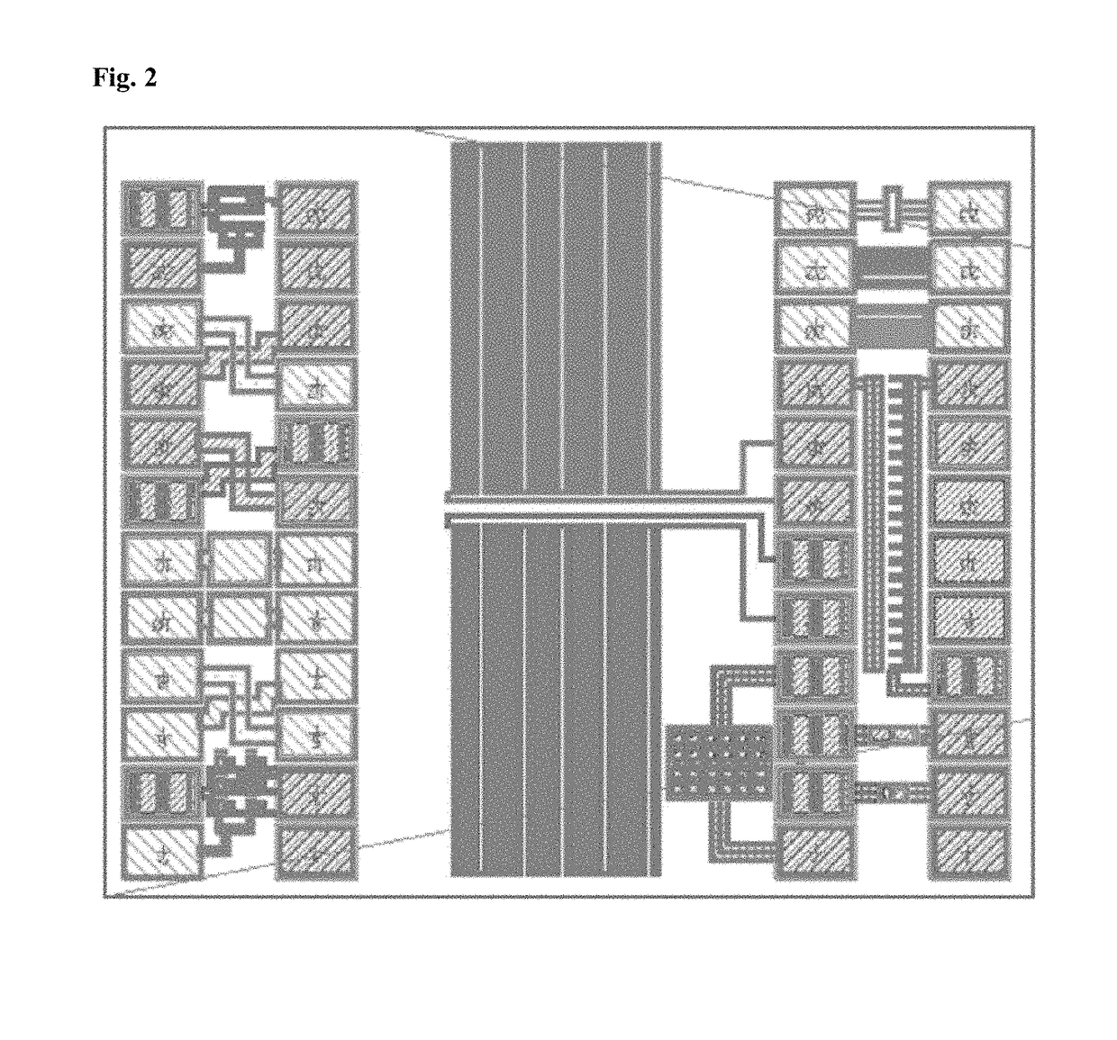
[0034]Reference will now be made in detail to the aspects of the present disclosure, examples of which are illustrated in the accompanying drawings. Whenever possible, the same reference numbers will be used throughout the drawings to refer to the same or like parts.

[0035]It will be understood that when an element such as a layer, a film, an electrode, a plate, or a substrate is referred to as being “on” or “under” another element, the element may be directly on another element or an intervening element may also be present.

[0036]Spatially relative terms, such as “below”, “beneath”, “lower”, “above”, “upper”, and the like, may be used herein for ease of description to describe one element or feature's relationship to another element(s) or feature(s) as illustrated in the figures. Elements depicted in the drawings are not necessarily to scale with one another, rather individual elements may be enlarged or reduced in order to more easily comprehend the elements in the context of the de...


PUM


Abstract

The present disclosure relates to an array substrate for an X-ray detector and an X-ray detector including the same. The array substrate is defined as an active area and a pad area, wherein the pad area comprises a plurality of test areas comprising a first test pattern and a second test pattern, the first test pattern comprises a first gate electrode on a substrate, a first active layer on the first gate electrode, a first source / drain electrode on the first active layer, and a first data line on the first source / drain electrode, and the second test pattern comprises a first lower electrode on the substrate, a first photoconductive layer on the first lower electrode, and a first upper electrode on the first photoconductive layer, thereby measuring the characteristic of each of a transistor and an optical detector with high accuracy.

Description

CROSS-REFERENCE TO RELATED APPLICATION[0001]The present application claims the priority of Korean Patent Application No. 10-2015-0191497 filed in the Republic of Korea on Dec. 31, 2015, which is hereby incorporated by reference in its entirety.BACKGROUNDField of the Disclosure[0002]The present disclosure relates to an array substrate for an X-ray detector and an X-ray detector comprising the same, and more particularly, to an array substrate for an X-ray detector and an X-ray detector including the same, for capable of separately measuring characteristics of a transistor and an optical detector of the X-ray detector with a high accuracy.Description of the Background[0003]An X-ray inspection method that has been widely used for medical diagnosis requires an X-ray sensing film and a film printing time to obtain a result.[0004]However, recently, by virtue of development of semiconductor technologies, a digital X-ray detector using a thin film transistor (TFT) has been researched and de...

Claims


Application Information

Patent Timeline
Patent Type & Authority Patents(United States)
IPC IPC(8): G01D18/00G01T1/24G01T7/00H01L27/146H01L21/66
CPCG01T1/241G01T7/00H01L27/14676H01L27/14612H01L22/34H01L22/32H01L27/14658H01L27/14663
Inventor YOON, JAEHO
Owner LG DISPLAY CO LTD
Why Eureka
Try Eureka